Good article on the history of Apple's SoC designs:
http://www.eetimes.com/electronics-...series-family--More-than-a-hobby?pageNumber=0
Viewing more than 2 pages is hidden behind a register wall, so I'll provide some choice excerpts.
The fact that Intel and AMD would be the only other full custom design entities out there should show you how expensive and resource intensive a full custom layout is.
This commitment to true custom design shows Apple's devotion to the ARM ISA and platform long term. It also shows their unwillingness to compromise on "good enough" performance and to always be the best they can be, even if the basis for comparison across platforms doesn't always exist in an easily interpretable way due to ecosystem and UI differences.
![O6i47Rp.jpg]()
A6 die shot
![pXHxRS3.jpg]()
A6X die shot
![Fak8jVc.jpg]()
A series family tree
It's interesting to note that there are significant design differences beyond the GPU cores and RAM interface, which were both known and necessarily needed to be different.
![HgygOOJ.jpg]()
Die size allocation of A series chips
It's important to note that die size can't increase perpetually. You start running into yield issues and cost per die that makes it uneconomical. Even if Apple didn't mind high cost and lower yield, they'd probably run into capacity issues, preventing further growth.
It's also unavoidable that power consumption increases with die size growth. Since the A4, peak power consumption on all major SoCs have more than doubled. Designs get away with this because the CPU is executing tasks faster and turning off quicker, but there's a wall here too. Eventually a power wall is hit and the only way you can squeeze more performance out is to go more custom (as apple has done), or simply wait for a process shrink. A lot of manufacturers have been hiding this increase with larger batteries, which apple hasn't done. Fairly consistent battery performance across iphone and ipad generations is certainly an accolade given this.
Anobit was related to NAND controllers (and specifically endurance). This would apply to both their mobile devices and their Mac lines.
Mobile GPU makers typically don't license their designs on an architecture basis. They usually have multiple core level offerings.
However, ImgTec does have a history of providing "custom" designs. The PS Vita has a SGX543MP4+, and the "+" has never been disclosed as to what it actually is. It could refer to their custom wideIO RAM interface, but no one has said anything.
ImgTec has divided their next generation Rogue cores into 2 lines: The G6200/6400/6600 are 2/4/6 "cluster" variants of the core. They also have 6230/6430/6630, which add special frame buffer compression logic*. (this would allow increased performance by allowing more data to be sent to the display with a given memory bandwidth, or alternately, less power as you reduce the memory bandwidth to get the same throughput. This is all at the cost of more die area, but Apple's mobile dies are among the biggest out there in the mobile world) It's possible this was an apple requested change that was turned into an alternate product line for ImgTec.
It's important to point out that Apple is a 10% stake holder in ImgTec, so none of this would be a surprise. ImgTec is also very well positioned as a company because they just acquired MIPS (alternate CPU licensing entity like ARM, but usually found in set top boxes) and Caustic (which produces custom ray tracing cards).
* source: http://forum.beyond3d.com/showpost.php?p=1703350&postcount=575
http://www.eetimes.com/electronics-...series-family--More-than-a-hobby?pageNumber=0
Viewing more than 2 pages is hidden behind a register wall, so I'll provide some choice excerpts.
Die photographs of the A6 and A6X that were first published by Chipworks, with our added annotations, are reproduced below. Probably the single most striking feature of both is the in-house designed CPU. Going further, it was a custom design where the layout was performed manually, instead of using the common automated place and route approach. In their discussion of the A6 ChipWorks commented: "This is a more expensive and time-consuming method of layout. However it usually results in a faster maximum clock rate, and sometimes results in higher density." They go on to say: "In fact, with the exception of Intel CPUs, it's one of the first custom laid out digital cores weve seen in years!"
The fact that Intel and AMD would be the only other full custom design entities out there should show you how expensive and resource intensive a full custom layout is.
This commitment to true custom design shows Apple's devotion to the ARM ISA and platform long term. It also shows their unwillingness to compromise on "good enough" performance and to always be the best they can be, even if the basis for comparison across platforms doesn't always exist in an easily interpretable way due to ecosystem and UI differences.
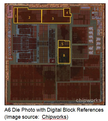
A6 die shot
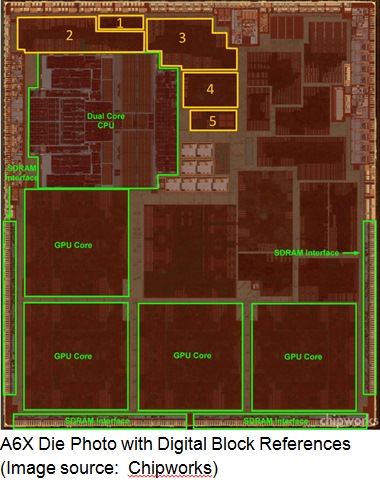
A6X die shot
Chipworks presented some quantitative numbers comparing the A6 and A6X, in their November 1st discussion of the A6X. With a die size of 124 mm², the A6X is 28% larger than the 96.7 mm² A6.
The CPU consumes 15 mm² on both parts, while the triple core GPU of the A6 weighs in at 16 mm², and the quad core GPU on the A6X comes in at 35 mm².
From the above numbers it is apparent that beyond the additional 19 mm² for the GPU the A6X sports approximately 10 mm² additional area. This may not seem like that much, but it is actually an area larger than the individual GPU cores.
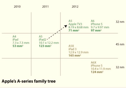
A series family tree
One can also look at this more quantitatively, yet without a large reverse engineering project. Of the five digital blocks (see die photographs) most easily identified between the A6 and A6X, four occupy areas between eight and 10 percent larger or smaller than on the A6. The differences are at the upper end of measurement errors (we are relying on CW published die dimensions and the accuracy of the associated image files posted on web sites), so are believed to represent minor design changes within the blocks. The fifth digital block analyzed varied significantly between the two designs. The A6X version of this digital block was just over three times that of the A6.
Getting back to processor cores for a moment, there are four GPUs on the A6X compared to three on the A6 (as noted by Chipworks). The design within each of these also differs significantly.
The GPU blocks on the A6 are 58% bigger than their A6 counterparts. Accounting for the GPU cores along with the block that could either be a dedicated decoder or perform a GPU load balancing operation, there is nearly twice the die area directly devoted to graphics processing on the A6X.
It's interesting to note that there are significant design differences beyond the GPU cores and RAM interface, which were both known and necessarily needed to be different.
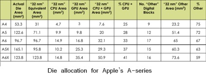
Die size allocation of A series chips
A number of things jump out from the table. First is the continued increase in 32 nm equivalent die size for both processor streams as seen in the third column.
The A6 was introduced during the September 2012 keynote as being 22% smaller than its predecessor. This is true on a silicon basis, but on a circuit basis i.e. corrected for the shrink, it is in fact 36% larger. The same is true for the A6X which is 29 % larger than its 5 level sibling.
There are quite a few more transistors on these parts. Looking within the die, the corrected CPU area is 50% larger with the custom designed cores on the 6 level parts. The area devoted to the GPU, on the other hand, has continually increased in the two streams.
It's important to note that die size can't increase perpetually. You start running into yield issues and cost per die that makes it uneconomical. Even if Apple didn't mind high cost and lower yield, they'd probably run into capacity issues, preventing further growth.
It's also unavoidable that power consumption increases with die size growth. Since the A4, peak power consumption on all major SoCs have more than doubled. Designs get away with this because the CPU is executing tasks faster and turning off quicker, but there's a wall here too. Eventually a power wall is hit and the only way you can squeeze more performance out is to go more custom (as apple has done), or simply wait for a process shrink. A lot of manufacturers have been hiding this increase with larger batteries, which apple hasn't done. Fairly consistent battery performance across iphone and ipad generations is certainly an accolade given this.
First, it will be interesting to see if the die size plateaus at some point.
Second, it will be interesting to see how the block count evolves going forward, with IP of the anobit or authentec acquisitions possibly showing up in future designs.
Anobit was related to NAND controllers (and specifically endurance). This would apply to both their mobile devices and their Mac lines.
Finally, the big one: Will there be an Apple designed GPU? It is clear that the GPU is continually consuming more silicon whether you look across the whole family our just within one branch. Based on the move to a custom CPU design this may well be in the back of their head. The question of sufficient engineering resources and/or graphics IP is a topic best left for another day.
Mobile GPU makers typically don't license their designs on an architecture basis. They usually have multiple core level offerings.
However, ImgTec does have a history of providing "custom" designs. The PS Vita has a SGX543MP4+, and the "+" has never been disclosed as to what it actually is. It could refer to their custom wideIO RAM interface, but no one has said anything.
ImgTec has divided their next generation Rogue cores into 2 lines: The G6200/6400/6600 are 2/4/6 "cluster" variants of the core. They also have 6230/6430/6630, which add special frame buffer compression logic*. (this would allow increased performance by allowing more data to be sent to the display with a given memory bandwidth, or alternately, less power as you reduce the memory bandwidth to get the same throughput. This is all at the cost of more die area, but Apple's mobile dies are among the biggest out there in the mobile world) It's possible this was an apple requested change that was turned into an alternate product line for ImgTec.
It's important to point out that Apple is a 10% stake holder in ImgTec, so none of this would be a surprise. ImgTec is also very well positioned as a company because they just acquired MIPS (alternate CPU licensing entity like ARM, but usually found in set top boxes) and Caustic (which produces custom ray tracing cards).
* source: http://forum.beyond3d.com/showpost.php?p=1703350&postcount=575