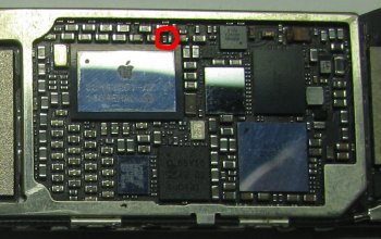
Happy apple day everyone. Time for one final prediction update going into the event. In my previous prediction, I took none of the PCB leaks into account for my guess. Now we've received visual information from the package that shows it's smaller size than the A7 as well as a silk screen code that shows LPDDR3 at 1600 MHz in size is still in use. Somewhat surprisingly, it's also only 1GB still. The codes don't give any clear indication as to whether the fab house is now TSMC. The smaller pinout suggests many possibilities, as was discussed in the original post. Keep in mind that package size and pinout don't maintain a fixed ratio to die size, however.
Last night, a geek bench test bench run on a purported iPhone 6 showed a 1.38 GHz clock frequency, a modest bump over the 1.3 GHz A7 as expected, along with a roughly 10% speed boost, clock for clock. This was expected based on the ambitiousness of the A7 design already. It also seems to have confirmed 1GB RAM again.
Without further ado, the new prediction:
A8 Prediction
A8
- Manufacturer - TSMC on HKMG 20nm process
- Die Size - 90-100 mm2
- Designer - Apple
- CPU Type - 1.4GHz Third Generation Custom Apple Core
- Core Count - 2
- Instruction Set - ARMv8-A (with custom Apple extensions)
- Chip Designator - S5L8970X
- L1 Cache - 64/64KB
- L2 Cache - 1MB
- L3 Cache - 4MB
- RAM - 1GB LPDDR3 @ 1600 MHz (64 bit interface, PoP for iPhone)
- Max Theoretical Memory Bandwidth - 12.8 GB/s
- GPU Type - "Hex Cluster" PowerVR GX6650 @ 450 MHz
- GPU Performance - 172.8/354.6 GFlops (FP32/FP16)

")