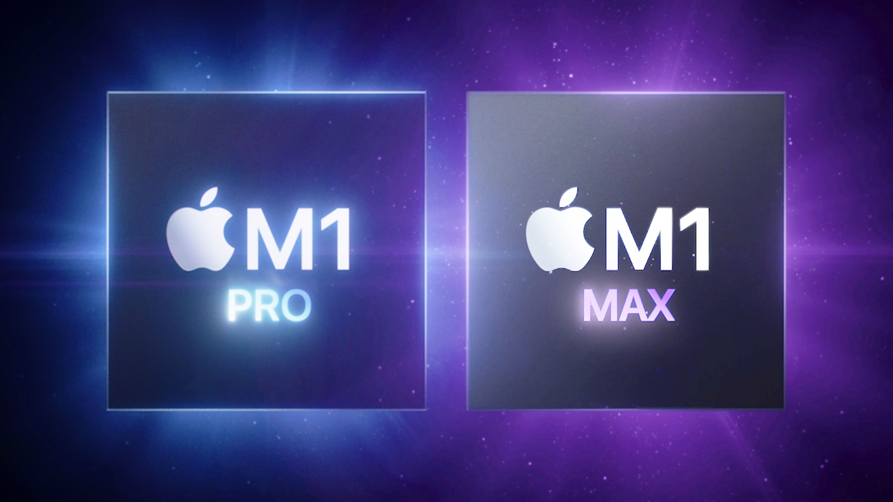
With Mac Studio it seemed to me that the UltraFusion Interconnect was used in that case to combine 2x M1 Maxes into the Ultra, but the actual power of UFI is giving customers ability to customise what kind of compute power the machine will be focussed on, even within the SoC architecture, rather continuing to double everything with "extreme".
The Ultra Fusion Interface is primarily a hyper local inter-die communication interface. It is contructed by putting two bigger dies on top of another small silicon die. ( InFO_LSI on the right below. UFI is plays the role of 'LSI' in that diagram )

AnandTech Forums: Technology, Hardware, Software, and Deals
Seeking answers? Join the AnandTech community: where nearly half-a-million members share solutions and discuss the latest tech.
It is not very likely that Apple is going to run off and create 3-4 different dies to mix-and-match with other dies.
Perhaps there is a small scale die that Apple 'spins out' that is PCI-e provision and just maybe does some
However, it is pretty doubtful they are going to 'rip' the cores they normally co-locate on die ( CPU , NPU , GPU , Impage process) out into an independent , homogenous die. If push too much memory traffic over the UFI connection it won't as well. By putting 'mega' memory bandwidth on each of the two medium-large dies in the Utlra package they cut down on the traffic that has to traverse UFI.
What is being over looked is that the two 'Max' dies cover up all ~10,000 connectors on the UFI LSI die. Pointing off to well other stuff is going to get hooked up is from where? Out the 'bottom' of the LSI off to other Package? Or just an indirect way of doing what InF
Folks are treating UFI like it is AMD's Infinity Fabric or Nvidia's NVLINK2 (or gen 3 ) and they may not be necessarily true. Fairly decent chance that UFI is 'fabulously' low power because it is super short range. Perhaps there is some re-drivers/signal boosters that could communicate to a shared PCI-e and/or secondary memory controller where they take the speed/latency hit , but probably not for huge direct memory bandwidth consumers like Appe's main types of cores.
Using the plain Mx to span MBA , MBP 13" , iMac , Mini it is pretty apparent that Apple is looking to do as few dies as they can get away with. The Ultra package using two 'Max' dies where the second die has a redundant secure enclave , some spare TB controllers , system management , etc. To do quad-die it probably would be effective to come up with a non exact matching 'twin' , but still 85+ % overlapping die design elements and layout. ( e.g, sub out secure element and some TB controllers for PCI-e lane provision). Then use one TB focus and one PCI-e focused die to get a Ultra like 'pair' ( could use that in a studio and just not provision out the PCI-e lanes internally) . An then two of those pairs to get to quad ). It they 're-use' most of the Max design then the R&D costs get spread out over more SoCs in more products. ( that has been Apple's modus operandi for their silicon SoCs for years now. Do a few types and spread them out over as many products as they can. )
Mac Pro probably gets something incrementally different. But probably won't be radically different.
So say every Mac Pro was build to order with an M1 Ultra as the base, but the UFI is extensible in a way that allows you to fill up to (say) 8 extra slots with chips that are some combination of dedicated CPU, GPU, RAM or neural engine modules, all connected to the M1 Ultra via UFI. If the performance is there, there might not be too much grumbling about lack of support for third party components.
Whatever is directly coupled to UFI is going to be "glued' to the package. I doubt Apple is going to do 'build to order' chip packages.
Apple probably provision some PCI-e so folks can put in cards into a Mac Pro. But their cores ... those will be embedded in the package. UFI doesn't open that up at all. It is meant for dies to be 'glued' on top.


