Become a MacRumors Supporter for $50/year with no ads, ability to filter front page stories, and private forums.

MacRumors

macrumors bot
Original poster
Apr 12, 2001
69,429
40,522


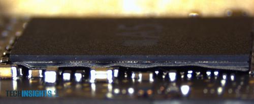
Side view of A5 package (UBM TechInsights)

A pair of chip teardown firms this weekend stripped down the new A5 system-on-a-chip used in the Apple's iPad 2, finding that the package is indeed being manufactured by Samsung. Several rumors in recent weeks have claimed that Apple is shifting production from Samsung to TSMC, and while that may still be the case for future production, Samsung is clearly responsible for early production runs.


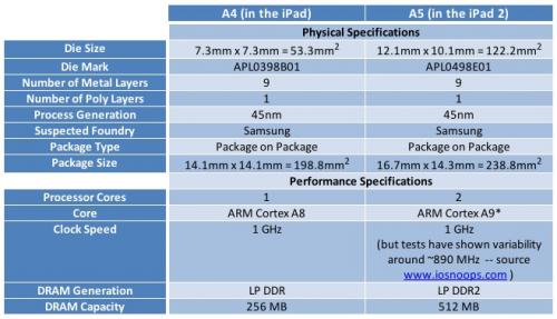
Comparison of A4 and A5 packages (UBM TechInsights)

UBM Techinsights performed a complete teardown of the iPad 2, with a special focus on decapsulating the A5 package.Based on analysis performed by UBM TechInsights Lab and Process Analysis personnel, we can say that the A5 in our possession is definitely manufactured by Samsung using their 45nm process. UBM TechInsights used optical die and SEM cross-section images to analyse important features such as die edge seal, metal 1 pitch, logic and SRAM transistor gate measurements. These features were then compared to other manufacturers in our database, including other Samsung 45nm parts. The previous generation Apple A4 processor was also fabbed on Samsung's 45nm process.UBM TechInsights also discovered that the A5 packages from two iPad 2 units used DRAM from two different sources, Samsung and Elpida, indicating that Apple has tapped multiple suppliers even for portions of the complex A5 package in order to meet demand.

094948-a5_chipworks_sem.jpg

Scanning electron microscope cross-section of A5 (Chipworks)

Chipworks has also performed a decap of the A5, similarly revealing that the package is being manufactured by Samsung.At this scale even electron microscopes start to run out of steam, so not the clearest of images in either case, but good enough to see the similar shape of the transistor gates and the dielectric layers. So at least this sample of the A5 is fabbed by Samsung, just as all Apple's processor chips have been for the last while.Also of interest, iOSnoops discovered that the while the A4 chip found in the original iPad clocked in at a consistent 1 GHz, each of the two cores in the new A5 seems to run at a variable speed between 861 MHz and 894 MHz depending on the app being run, suggesting that Apple has built in more advanced power management features for the A5.

Article Link: Chip Teardown Firms Confirm iPad 2's A5 Chip Manufactured by Samsung
 
only 894Mhz??
Its not a real issue for me but I figured Apple would put some limitation for the 10 hour battery life
 
...

I highly doubt the power management can only scale from 861 to 894. That would be useless.
 
Sure SEM or TEM ? Buyers tip - hold off on JEOL for a while.

As I side note - I hate it when scales are not included with photomicrographs. What's the point without them?

Agreed, they should include scales with the images.
 
Interesting how there is variable power to preserve battery. I'm actually mildly surprised by that spec.
 
I highly doubt the power management can only scale from 861 to 894. That would be useless.

Totally agreed, we all need that extra 139 to 106 mhz.

I notice it every time I look at how this version ipad doesn't somehow perform right.

Such a shortcoming would not happen on a Xoom.


Paaaaallleeeeeezzzzeee!
 
People have quoted detected speeds over 900MHz as well. There's no reason to believe anything other than the A5 being variable up to 1GHz. Other CPUs have been doing this kind of load-based frequency adjustment for quite some time.
 
The A5 has 2.3x the die size of the A4 and the package is only 20% bigger. It looks like they conserved space in both the chip itself and in the iPad 2 with its weight and volume loss.

Apple is trying to get 28nm dies for the A6 vs 45 nm now, a 37% reduction. It appears the A6 may comfortably have 4 cores, a gig of memory, and integrated GPU(s) in addition to likely 200-400 mhz bus(es) and a 1ghz frequency range.

March 2012 iPad 3 and LTE, here we come. :D

Rocketman
 
Last edited:
It seems to be an advanced chip that a system to adjust speed for battery consumption. Kinda like optimus thing that uses two different graphic cards: discrete vs integrated (?). This is a cool chip;)
 
The A5 has 2.3x the die size of the A4 and the package is only 20% bigger. It looks like they conserved space in both the chip itself and in the iPad 2 with its weight and volume loss.

Apple is trying to get 28nm dies for the A6 vs 45 nm now, a 62% reduction. It appears the A6 may comfortably have 4 cores, a gig of memory, and integrated GPU(s) in addition to a likely 200-400 mhz bus and a 1ghz frequency range.

March 2012 iPad 3 and LTE, here we come. :D

Rocketman

When you shrink the minimum feature size by 62%, obviously the die size decreases by much less (since few features are drawn to the minimum feature size and things like metal thickness don't scale proportionally, necessitating maintaining large distances between metal to prevent parasitic coupling, etc.)


It seems to be an advanced chip that a system to adjust speed for battery consumption. Kinda like optimus thing that uses two different graphic cards: discrete vs integrated (?). This is a cool chip;)

Not at all like that. It just throttles the clock, like speedstep and powernow have done for a decade, and like has been done by other chips at least as far back as 1996.
 
There's enough room to at least keep the same overall density and add two more layers to the chip, plus if they increase the chip size itself again another 20%, that makes for a ton of room for fancy electronics to disect in another year.

It might run nice in an iPad 3 also, but who cares about that when you can tear the thing down. :)

When you're done I suppose you can blend it too.

Rocketman
 
People have quoted detected speeds over 900MHz as well. There's no reason to believe anything other than the A5 being variable up to 1GHz. Other CPUs have been doing this kind of load-based frequency adjustment for quite some time.

+1, I'm literally in shock at how blogs and sites keep reporting the 894-900mhz figure without really thinking it through. I swear I thought we were dealing with intelligent people. I swear I did.

Its a 1ghz proc. It can reach 1Ghz.
 
+1, I'm literally in shock at how blogs and sites keep reporting the 894-900mhz figure without really thinking it through. I swear I thought we were dealing with intelligent people. I swear I did.

Its a 1ghz proc. It can reach 1Ghz.

It doesn't matter if:

  • It hasn't been tested to that speed, because Apple wanted to pay less and/or have higher yields.
  • There's no intention to go that high, because of battery conservation.
People get way too hung up on theoretical speeds.
 
+1, I'm literally in shock at how blogs and sites keep reporting the 894-900mhz figure without really thinking it through. I swear I thought we were dealing with intelligent people. I swear I did.

Its a 1ghz proc. It can reach 1Ghz.

The technology realm has not been primarily populated by intelligent people for over 20 years now.
 
+1, I'm literally in shock at how blogs and sites keep reporting the 894-900mhz figure without really thinking it through. I swear I thought we were dealing with intelligent people. I swear I did.

Its a 1ghz proc. It can reach 1Ghz.

What do you want them to do? Lie and say it runs at 1GHz to make you happy? This is nothing new, Apple is more concerned with battery life than speed.
 
Register on MacRumors! This sidebar will go away, and you'll see fewer ads.