Become a MacRumors Supporter for $50/year with no ads, ability to filter front page stories, and private forums.
Now if youre saying that the PCB layout has not been proven and I need to test it when one arrives...thats as simple as doing what I do with my handmade ones. Unless I missed the question?
I meant testing the assembled boards before insertion into equipment.

Even well-manufactured boards can have defects. Some boards I was using recently had a short that drove a uC pin to -4V. Not good. The defect was on the board, a tiny unetched short where a trace passed a pad. Thankfully it was a one-off defect, but I had to test my remaining boards to make sure. I only found the defect because I wrote the firmware to produce test signals and a rudimentary self-test when told to do so. It's not fancy, just blinkenlites, but it's easy to tell by the blink pattern whether it's working or not.


There really is no need to mount or attach this board to anything, it fits snug enough in the space (but not too snug, I tested a cut out print of the PCB) I am not worried about jiggling or shorting.
Well, you didn't say anything about mounting before, which is why I mentioned it. Newbies have been known to leave things out, and you did say you were a newb at this.
 
Im hoping, as most probably do, to get this PCB done right the first time and have a minimal amount of duds. Making this PCB allows me to know that at least my wiring setup is not to blame when it doesnt work. (after testing the boards for proper continuity)

And on a side note, some of the "auto" route choices it makes sometimes are ridiculous. One time it gave me like 5 VIAs for a single wire...for no reason!?
 
Last edited:
IMO you should consider using thru hole sockets for the external connectors, screw terminals or similar.
 
is a through hole going to have a smaller or larger footprint than these solder pads?

It should depend on what kind of sockets you use, look in the component library and see if you find some known brands and try it out. Molex has some snap in ribbon connectors for example, that has a smaller footprint than screw terminals. By just eyeballing what you got there I'd say it should be about the same. Even if you don't use a socket though, you should be able to pick a through hole solder pad as it's easier to solder. Just my opinion however, someone else can perhaps chip in and give their opinion as well.
 
Last edited:
And perhaps less chance for shorting errors?

But...wouldnt I have to be using a very thin wire I could insert into the hole for soldering much like a thru hole component?

The smallest hole I found is:
THROUGH-HOLE PAD
Package: 1,6/0,8

And if im not mistaken, 0.8mm is pretty small for even thin wire to pass thru.
 
Last edited:
I guess it would not come down to layout, but the fact that it's easier to solder in that case.
 
Wirelessly posted (Mozilla/5.0 (iPhone; U; CPU iPhone OS 4_3_2 like Mac OS X; en-us) AppleWebKit/533.17.9 (KHTML, like Gecko) Version/5.0.2 Mobile/8H7 Safari/6533.18.5)

The pads for your PIC and SIP and transistor are "standard" 0.1" push through pads. ;)

What gauge are the wires you are interfacing with?

B
 
24ga from CAT5 cabling which is a little more than 0.5mm

so i guess 0.8mm drill size is just fine.

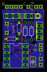
Hmmm. Is solder pad a the ONLY choice you have when doing a double sided board so as to not have issues using a thru wire like this? I had to move one of the blue wires from below a solder pad which I turned into a hole.
rgedhkl.jpg
You can see by the S in the lower right, I added a kink to the blue line which runs up to the right.

Still debating removing the blue fill from under all solder holes.

And is it ok to get in the only error from ERC which says some components have no value? I did give values when doing the schematic, but the labels were getting in the way during PCB (and I know the values) so instead of turning off that layer, I deleted the value entirely...oops?
 
Yeah, therein lies the rub. a through hole limits your routing even on a dinky 2 layer board. Yet another reason I prefer SMT. :p Pulling back your ground fill around the holes is perfectly reasonable.

Personally, I'd like to see a bit more metal around those wire holes similar to what you have around the DIP parts. You want to have enough room for the solder to be to enable a good connection. I tend to lay the loose end of the wire down and get some more contact area.

If you stick with the wire holes I'd also strongly recommend using a standard pitch (if possible) either 0.1" or 2 mm if possible so that you have the option of sticking a header in the holes too.

Again, I think that for the most part I'd go with wider traces on the board aiming for 0.5 mm or ~0.020" in all the power traces and anything that takes power.

B
 
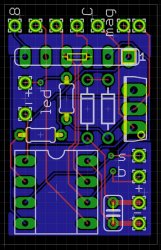
I think this is the best I can do with the components and space limitations I have. Much more movement seems to really throw off routing something crazy. And in some cases doesnt really allow for 45° turns at all.
Screen-shot-2011-07-09-at-12.22.jpg
Though I might move one of the mag connections over.
 
Got my PCBs back from the printer...totally awesome.

Everything works great and I am very pleased.

Thanks to everyone who helped me make the best out of it. Especially the guy who said holes instead of solder pads.

:D
 
Awesome!

Quick note if you respin. Current flows from your power source beyond that first cap, if possible, fatten those traces too. ;)

B
 
Register on MacRumors! This sidebar will go away, and you'll see fewer ads.