Become a MacRumors Supporter for $50/year with no ads, ability to filter front page stories, and private forums.

MacRumors

macrumors bot
Original poster
Apr 12, 2001
63,407
30,563


Since the Apple Watch's initial unveiling last September, Apple has touted the S1 chip that serves as the brains of the device, with the company noting is has essentially packed an entire computer onto a single ultra-compact chip that is encapsulated in resin to help protect it from the elements.

iFixit was unable to delve into the S1 itself in the firm's initial teardown of the Apple Watch, and Chipworks offered an early look at the chip's internals starting x-ray imaging, but now ABI Research has more fully deconstructed the S1 and identified a number of its components.

s1_decapped_abi.jpg
ABI's photo shows the center of the S1 dominated by the main processor carrying part number APL 0778, with 4 Gb (512 MB) of Elpida SRAM on top. We've yet to see a detailed look at the internals of the main processor, which should provide yet another interesting look at a custom Apple chip design when it does surface.

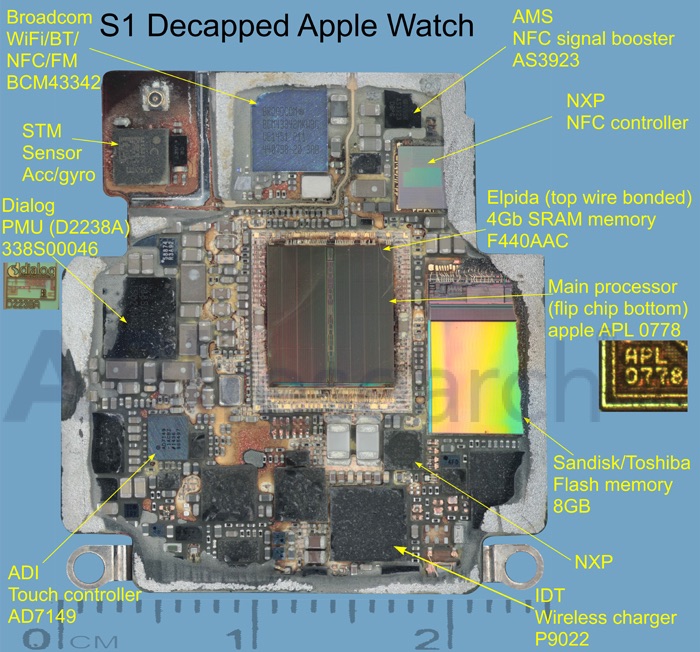
Also included on the S1 are an 8 GB flash storage chip, the Broadcom Wi-Fi chip cleverly identified by Chipworks from Apple's promotional footage last September, an accelerometer/gyroscope from STMicroelectronics rather than the predicted InvenSense, touch controllers unexpectedly from ADI, and a wireless charging chip from IDT to facilitate the Apple Watch's inductive charging.
"The design is an obvious variation from Apple's smartphones, with many high-end functions / chips included that normally would not be found in a simple watch," comments Jim Mielke, VP Engineering at ABI Research and head of the TeardownIQ group. "Judging by the complexity of the printed circuit board (PCB), and the number of parts on the PCB, one might think the Apple watch is a full-fledged cellular connected watch but in fact connectivity is limited to Wi-Fi, Bluetooth, and NFC."
In its initial look last week, Chipworks highlighted the 6-axis accelerometer/gyroscope, which marks the first time Apple has been able to include all of that functionality in a single component.

s1_xray_chipworks.jpg
This is the first time that we see a true 6X sensor in an Apple product that doesn't require an external accelerometer. In the iPhone 6 and 6+ we saw an Invensense 6 axis sensor and a Bosch 3 axis accelerometer. Here in an even more compact design, the Apple Watch, we finally have a solution for all 6 axis in a single component.
As seen in iFixit's teardown, the S1 is a remarkably compact chip taking up a small percentage of the overall device volume in laying flat in the bottom of the casing. The majority of the space inside the casing is taken up by the battery and Taptic Engine/speaker assembly. We expect to see more details on the S1, particularly the main processor, in the coming days as chip experts get closer looks at the part.

Article Link: Early Looks Inside Apple Watch's S1 Chip Confirm 512 MB RAM, Unexpected Suppliers
 

Phil A.

Moderator emeritus
Apr 2, 2006
5,799
3,094
Shropshire, UK
It's an amazing bit of engineering, but IMO creating a tiny circuit board with normal components on it and then covering it in epoxy does not make it a single chip
 

mattthecoolguy

macrumors newbie
Mar 12, 2015
18
35
Wow that's impressive. Has anyone figured out the size (mAh) of the battery in the 42mm version? I know that they figured out the size of the 38 when iFixit tore it down, but I haven't heard anything about the 42.
 

lincolntran

macrumors 6502a
Jan 18, 2010
843
471
512 RAM is a lot for a watch! I think the 1st version of the watch is a lot more capable than the first iPad. That means it will be able to run independent apps once Apple open that out later this year!! The hardware is ready, just waiting for watch OS to catch up!
 

Mhkobe

macrumors regular
Jun 25, 2009
140
0
Should Say DRAM not SRAM

Like it says in the title, the "4Gb SRAM" should say "4Gb DRAM".
 

FX120

macrumors 65816
May 18, 2007
1,173
235
It's an amazing bit of engineering, but IMO creating a tiny circuit board with normal components on it and then covering it in epoxy does not make it a single chip

This has been bothering me since they announced the watch. Calling it a 'chip' implies its a single wafer, or a SoC which this is not.
 

/dev/toaster

macrumors 68020
Feb 23, 2006
2,478
249
San Francisco, CA
"4 Gb (512 MB)" - what does this mean?

I don't understand why it was written like that .. very confusing.

----------

Gb written with a lowercase 'b' means GigaBITS.
GB written with an uppercase 'B' means GigaBYTES.

4 Gb is really 512MB (4 GB divided by 8 - 8 bits in a byte)
4 GB is really 4 GB

I don't think I have ever seen RAM written as Gigabit before ... that's so strange.
 

ZCT

macrumors 6502
Sep 15, 2014
358
173
Minneapolis, MN
Wow, that looks so basic and straightforward. I could have designed that in my lunch break.

Yeah, clearly Apple are ripping us off with this DISGUSTINGLY over priced watch at $349. Damn that Tim Cook and his evil greed.

:rolleyes:
 

PBG4 Dude

macrumors 601
Jul 6, 2007
4,264
4,471
The actual chips are measured in the number of bits, in this case, gigabits, are on the chip. Seems to be an industry norm when discussing the actual chips themselves.
 

PBG4 Dude

macrumors 601
Jul 6, 2007
4,264
4,471
Wow, that looks so basic and straightforward. I could have designed that in my lunch break.

Yeah, clearly Apple are ripping us off with this DISGUSTINGLY over priced watch at $349. Damn that Tim Cook and his evil greed.

:rolleyes:

Guess we're looking at the DJI Phantom's brain in about 5 years. :)
 
Register on MacRumors! This sidebar will go away, and you'll see fewer ads.