Become a MacRumors Supporter for $50/year with no ads, ability to filter front page stories, and private forums.
Apple's MCM patent cites off-loading I/O from the main die as one of the benefits of moving to MCM packaging.

Not suggesting this is happening, but loosely, to evaluate areas based on the current Max and the Reticle Limit in theorist9's post, a monolithic MCM Ultra sized die might be a possibility . . .

Monolithic Ultras.jpg


These layouts vaguely assume they'd sit with 2x the I/O of a Max given the current Mac Pro, but in MCM packages the I/O chips could be varied accordingly anyway.

Something interesting about the concept of pushing out a considerably larger MCM die for their desktops (which could land anywhere between the Max and the reticle limit), is that Apple's Patent clearly addresses x2 and x4 MCM configurations. Maybe the x4 is still a technical hurdle, but if they do manage to cover off the Ultra category with just one MCM die, and an x2 MCM config becomes the equivalent of their unrealised Extreme, then the prospect of a future x4 config would still be floating in the wind . . . tantalising?

The layout at the right of the Max shows about where the previous UltraFusion SOC only approach would hit the wall in terms of area. Something, as suggested by others, would need to be cut down from the default x2 Max for the Ultra.
 
Why do you think that is likely?

If you're thinking of Apple doing this to complement the work they are doing to catch up on AI in their next *OS, that's unlikely - the design of these chips were done a long time ago. Of course, it's likely to feature improvements to the Neural Engine anyway as it does every year.
The competition (Intel AMD and now Qualcomm) are increasing the TOPS of their NPUs. Qualcomm and AMD will soon offer 40-50 TOPS. Intel will follow with Lunar Lake and later. Apple is at risk of being perceived as falling behind the competition on the AI front. M4 likely hasn’t entered mass production yet so there’s still time to tweak the NPU design if Apple hasn’t done so already.

And on the thunderbolt side of things we all heard the announcement last year. So it’s reasonable to conclude that m4 will adopt it.

So if m3 ultra doesn’t have these features I’d say skip it as the next generation likely will.
 
Sorry, I'm confused. How does this fit with the internal bitmap having previously been 110 pts/in, changing to 127 pts/in when they switched to Retina displays?

If I understand the question correctly, that's orthogonal to the whole Retina stuff.

The last pre-Retina 15-inch MacBook Pro was available in 1440x900 at 15.4", i.e. 110 ppi, or as a BTO option in 1680x1050, or 129 ppi. The first Retina was 220 ppi, so it went back to 110 (times two) only. That's also true of the Touch Bar generation. The M1 Pro design indeed went up to 127 (times two).

Keep in mind higher ppis, especially at Retina, also make non-native resolutions less blurry. The more physical pixels there are, the less you are going to notice the upscaling/downscaling.
I'm afraid I don't understand what you're saying here, or how it relates to the question I asked. I was asking about the internal bitmap, the rendering, and the resampling, and you responded by saying developers develop against 72 DPI. I don't see how the latter relates to the former.
 
Equalising distances is another aspect of the MCM patent . . . so I'm guessing the GPU scheduler (GPU Misc.) will consolidate and move on to the central die of the MCM packages?

M3 MCM U:E.jpg


A die similar to the default (laptop) Max, just with a little more grunt for the desktop / MCM configs, seems more inline with Apple's GPU scheduler and MCM patents . . .
 
Last edited:
  • Like
Reactions: Antony Newman
Equalising distances is another aspect of the MCM patent . . . so I'm guessing the GPU scheduler (GPU Misc.) will consolidate and move on to the central die of the MCM packages?

View attachment 2364694

A die similar to the default (laptop) Max, just with a little more grunt for the desktop / MCM configs, seems more inline with Apple's GPU scheduler and MCM patents . . .
Technically interested but what about economics of scale? Is there enough potential market for an MxUltra (or Extreme) to justify the design, layout, testing and production of a chip? It seems, for Apple, custom chips require an application in a mobile device (phone, tablet, or laptop). The desktop market by itself is insufficient for the development of specialized custom processor chip.

A potential way forward could be a more in-depth application of chiplets, where high end desktop [continue] to use chiplets developed for other platforms but in greater quantities.
 
If the Mac Studio is capable of 370w, an M2 Ultra maxes out at 295w, and an M3 Ultra would need at least an additional 80w over the M2Ultra - could Apple have just painted themselves into a new (trashcan) thermal corner?

If TSMC N2 uses 30% less power - it would conceivably allow 30% more transistors; enough for an M4 Ultra in the Studio perhaps; But a full size Mac Pro might be required to quietly expel all the additional heat.

Also wondering if Apple would have to up the bandwidth of Ultrafusion from (bidirectional) 2.5TB/s if their MCM scheduler potentially connect to 4 SoC’s.
 
If the Mac Studio is capable of 370w, an M2 Ultra maxes out at 295w, and an M3 Ultra would need at least an additional 80w over the M2Ultra - could Apple have just painted themselves into a new (trashcan) thermal corner?

I imagine the mini/Studio is easier to embiggen if needed.

But… I’m also unsure why they couldn’t have done that with the trash can.
 
  • Like
Reactions: Tagbert
If the Mac Studio is capable of 370w
Lot depends on what limits the studio to 370W. If it is just the power supply itself, then boosting the power supply 25-40% (up to ~ 500W) is pretty straightforward and low risk, although with more noticeable fan noise. But if the 370W is the maximum cooling capacity, that could be a more complex issue.
 
  • Like
Reactions: Antony Newman
Technically interested but what about economics of scale?

Right or wrong, the current speculation assumes the existing M3 Max isn’t equipped to become an Ultra. This could be wrong, the lack of an interconnect may just mean the current M3 Max has something else going on that’s yet to be documented. The second part of this story is the premise and ‘supposed’ leak that the M3 Ultra will have no E-Cores, meaning it's unlikely to be comprised of 2x Max.

So yeah, not much really, but we also know from Apple's Patents that they are looking at MCM packaging to enable the x2 and x4 configurations needed for their A/Si desktop / workstation machines.

A monolithic Ultra does not seem likely, or possible, for all the reasons already cited in this thread, but I don’t expect Apple has proceeded onto the field with their own silicon just to forfeit the second half either. I expect the transition will be complete once the footprint of their M Family includes a chip purposefully intended for their desktop machines.

I’m not a beancounter, but they already have an architecture that serves every category of their product line. And it has the thermal headroom for them to produce workstation class machines with considerably reduced material (physical) footprints to their competitors.

There are considerable economies already built into Apple’s strategy. I think the question is, can they produce compelling enough machines, in terms of performance per dollar, to win back a good and viable portion of the workstation market going forward?

I’m betting yes! Mostly because I don’t like the alternative. I also tend to think they simply have to maintain their top tier machines for the sake of the whole stack . . .

I did contemplate shifting to Revit from my current B.I.M. a few years back. That had me looking at Windows workstations, but after 25 years on Apple . . . it wasn’t a solution I could stomach, not in terms of the OS or the branded boxes available and there was no real cost advantage over the then Intel Mac Pro. Apple has a chance to shift the performance per dollar equation well into their favour now with Apple Silicon.

The MCM die / chip layout above is just a compilation of what’s visible, to my understanding, of Apple's patents, with a dash of hopeful anticipation :). A 48 core GPU as the basis of their MCM desktops, would allow the Ultra to pull up beside a RTX 4090 for rendering workflows and an Extreme would be the equivalent of 2. That’s where I hope they are aiming, and land, with their M3 Desktops.
 
Last edited:
  • Like
Reactions: Antony Newman
Equalising distances is another aspect of the MCM patent . . . so I'm guessing the GPU scheduler (GPU Misc.) will consolidate and move on to the central die of the MCM packages?
I see two potential problems with this. First, we (or at least I) don't know what the bandwidth requirements are between GPU cores and "GPU Misc", and if it's large (my WAG says yes) then that's probably not practical. They already need a huge amount of bandwidth for cross-chiplet GPU traffic for it to be practical to access it as a single GPU in software.

The other problem is, possibly, insufficient shoreline to implement UltraFusion v2. Especially in the x4 configuration. But I guess they're going to have to solve that anyway. Which solution may well involve pushing some of the IO back out from the central die...

OTOH I do see some possibilities (possibly due to ignorance of GPU internals, so I welcome corrections): Tensor and matrix processor complexes may demand less bandwidth to the rest of the GPU, so perhaps they could be pulled out into a central chiplet. ...though that chiplet would then likely want to be on a leading-edge process as well, rather than falling back to N5 or bigger. Perhaps that's even an excuse to put the NPU on the central chip? That avoids duplication of NPU resources, which currently seem to be going to waste (AFAIK).

I also see another potential path forwards: Separate the CPU and GPU again! After all, on an existing Ultra, the CPU cores already have a 50% chance of not sharing a chiplet with any GPU cores they share a working set with. Perhaps the benefits of unified memory come mostly from shared address space (and maybe SLC?) and less so from both being physically close to the same RAM. Then you have to ask, do you want memory hanging off your CPU chiplets or your GPU chiplets? Or - if the system is smart enough about allocation, which I know Apple's been thinking about - maybe the answer is both.

If the Mac Studio is capable of 370w, an M2 Ultra maxes out at 295w, and an M3 Ultra would need at least an additional 80w over the M2Ultra - could Apple have just painted themselves into a new (trashcan) thermal corner?

If TSMC N2 uses 30% less power - it would conceivably allow 30% more transistors; enough for an M4 Ultra in the Studio perhaps; But a full size Mac Pro might be required to quietly expel all the additional heat.

Also wondering if Apple would have to up the bandwidth of Ultrafusion from (bidirectional) 2.5TB/s if their MCM scheduler potentially connect to 4 SoC’s.

M4 won't be on N2. For that you wait for M5. M4 is likely on N3E, possibly N3P. In fact if I had to bet right now, I'd say N3E for A18 & M4, and N3P for Pro, Max, and Ultra/whatever, though that will depend on shipping schedules- N3P won't be ready in time for A18 volumes, and possibly not for M4. If Apple pulls M4 Pro/Max into the same announcement as M4, N3P becomes a lot less likely.

As for Ultrafusion, clearly they'll want to maximize bandwidth to the extent economically possible. nVidia has now drastically surpassed Ultrafusion in bandwidth (either 2x or 4x - it depends on whether the quoted 10TB/s is summed both directions or not), so clearly there's room for it to grow, but nVidia can afford a lot more for this than Apple likely wants to spend, in both $$ and power.
 
  • Like
Reactions: Antony Newman
Technically interested but what about economics of scale? Is there enough potential market for an MxUltra (or Extreme) to justify the design, layout, testing and production of a chip? It seems, for Apple, custom chips require an application in a mobile device (phone, tablet, or laptop). The desktop market by itself is insufficient for the development of specialized custom processor chip.

A potential way forward could be a more in-depth application of chiplets, where high end desktop [continue] to use chiplets developed for other platforms but in greater quantities.
I was going to say that this has already been discussed a lot (including by me) in this thread and elsewhere.

But I realized recently that there's another possible answer. I don't really believe it, but it's not impossible.

That answer is, Apple could finally be ready to make a big play for the higher end market - the way it looked like they were in 2019. Of course the market has moved in a number of ways since then, and Apple has lost even more of the little trust they had left, so they'd have to understand that this is likely a decade-long play, with poor ROI in the first five years at least.

In all the discussions I've seen here (and elsewhere), it's been mostly assumed that Apple might be ready to take one step past the Ultra, maybe, and that's all. As name99 has pointed out a bunch of times, they've done at least some of the work necessary to go way past that point. If they're ready to go there, all bets are off.
 
I see two potential problems with this . . .

Thanks for the reply. Unfortunately I am in no position to correct anyone’s ignorance on GPUs or CPUs. I’m mostly here in anticipation of a faster machine, soon hopefully!

The layout was a question, and response, based mostly on the subject of die area raised in this thread, with some (very) basic interpretations of the various aspects articulated in Apple’s MCM patent.

You’ve raised a couple items / problems though, shorelines and bandwidth, which are mentioned in the background / overview of Apple’s patent, and for which they are proposing their MCM approach will provide a new solution. Not suggesting this means anything in terms of the layout above, but I am curious how Apple’s likely to push the envelope now that they appear to be defining and refining their M chip tiers . . .

  • 0020]
    In one aspect it, has been observed that for large MCMs, accommodating die-to-die routing between a large number of dies becomes more difficult to support due to limited wiring line space and via pad pitch in the MCM routing substate. This can force lower wiring counts and require higher data rates to achieve a target bandwidth. These higher data rates in turn may require more silicon area for the dies, larger shoreline to accommodate input/output (I/O) regions and physical interface (PHY) regions (e.g. PHY analog and PHY digital controller), more power, and higher speed Serializers/Deserializers (SerDes) among other scalability challenges.
  • [0021]
    In accordance with embodiments routing arrangements are described in which significant wiring count gains can be obtained, allowing the data rate to be lowered, thereby improving signal integrity, reducing energy requirements, and a potential reduction in total area. In accordance with embodiments, bandwidth requirements may be met by expanding die-to-die placement for logic dies, which would appear counter-intuitive since increased distance can increase signal integrity losses. However, the expanded die-to-die placement in accordance with embodiments can provide for additional signal routing, thus lowering necessary raw bandwidth. Additionally, signal integrity may be preserved by including the main long routing lines (wiring) in a single dedicated metal routing layer, while shorter signal routes between neighboring dies can use two or more metal routing layers. The additional signal routing can be achieved in multiple metal routing layers, which can also allow for finer wiring width (W), spacing (S) and pitch (P), as well as smaller via size. Furthermore, the routing substrates in accordance with embodiments can be formed using thin film deposition, plating and polishing techniques to achieve finer wiring and smoother metal routing layers compared to traditional MCM substrates. In accordance with embodiments additional signal routing requirements can also be met using a die-last MCM packaging sequence. In a die-first packaging sequence the dies can be first molded in a molding compound layer followed by the formation of the routing substrate directly on the molded dies. In one aspect, it has been observed that a die-first packaging sequence can be accompanied by yield limits to the number of metal routing layers that can be formed in the routing substrate. In a die-last packaging sequence a routing substrate can be pre-formed followed by the mounting of dies onto the pre-formed routing substrate, for example by flip chip bonding. It has been additionally observed that a die-last packaging sequence may allow for the combination of known good dies with a known good routing substrate with a greater number of metal routing layers, facilitating additional wiring gain counts.
  • [0022]
    The routing arrangements in accordance with embodiments may support high bandwidth with reduced data rates. This may be accomplished by increased wiring gain counts obtained by both expanding chip-to-chip placement and a die-last MCM processing sequence. Additionally, signal integrity can be protected by lower power requirements, and routing architectures in which main long routing lines between logic dies can be primarily located in a single dedicated wiring layer in the routing substrate, while shorter signal routes between neighboring dies can use two or more wiring layers. This may be balanced by achieving overall approximate equal signal integrity.
 
They are quite good at building GPUs, considering how much of the headstart Nvidia had. In some key areas (instruction scheduling, resource allocation, ALU utilization) Apple is ahead of Nvidia. I mean, we have Nvidia engineers openly saying that Apple managed to achieve things Nvidia tried and failed. There is a lot of evidence that Apple is building a superscalar GPU. It’s all quite exiting stuff for me as GPU tech enthusiast. In fact, I think that the GPU division is innovating at a much higher pace than the CPU division.
Yeah true that. As someone who has much more use for CPU power than GPU power, the only thing that doesn't make me yawn with each new M-chip generation, is the extra battery life.

For GPU power, the base M1 chip is overkill for my needs. Give me more CPU, RAM, and battery life though. And by CPU, I don't mean more cores, that's only helpful if the application can multithread enough to get use out of it. Graphics and AI can multithread to the end of the earth. Software compiling is much more limited.
 
Someone should tag MaxTech here and ask them to explain in more detail. Wouldn’t be surprised if they just evade scrutiny. Last time they posted on the thread that had their single NAND video, they conveniently stopped posting when directly challenged.
Hi @boak! What did you want to ask? To explain this article in more detail?

Here are some more thoughts:
M3 Max is the first Max die without the UltraFusion interconnect. You can see it for yourself in this additional die image which shows the M1 Max on left, M2 Max in the center, and M3 Max on the right. You can tell the UltraFusion connector is gone because the memory interface touches the bottom of the die.
Screenshot 2024-03-27 at 12.20.49 PM.png


What does this mean? It's either one of two options.

1. Apple decided not to release an M3 Ultra chip at all and wait for the M4 series, so they didn't need to print the UltraFusion connector at all.
2. They decided to completely redesign the M3 Ultra die.

This makes sense because the Ultra would no longer be dependent on the design of the Max dies, allowing them to fully customize the core layouts to what makes sense for high-end Mac Studio machines.

Why? Well, because the M1 Ultra and M2 Ultra chips suffered from terrible performance scaling, likely because of having to depend on the UltraFusion interconnect which isn't as efficient as higher all of the cores on the same die.

Example in 3DMark Wild Life Extreme Unlimited:
M2 Pro 16-core GPU FPS per core: 67FPS
M2 Max 30-core GPU: 124 FPS
M2 Ultra 60-core GPU: 222 FPS

Almost perfect 2x scaling from M2 Pro to M2 Max, but going from M2 Max to M2 Ultra is only 79% faster.

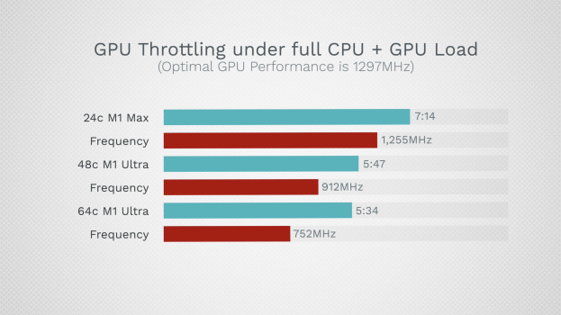
Not only that, but Apple's biggest struggle was pushing enough power to the M2 Ultra's GPU to keep the GPU frequency up. For some reason, with the M1 Ultra, as you added more cores, the GPU frequency would drop in our CPU+GPU torture test:
screenshot-2024-04-04-at-1-15-17-pm-png.2365582

It clearly wasn't limited by temps, because as we added more cores, the temps for both the CPU and GPU actually went down. Something else was bottlenecking the system. I believe there was some sort of an unexpected total power limit within the dies themselves, not having enough power to fire up all of those cores.
Screenshot 2024-04-04 at 1.15.26 PM.png


Because of this, Apple could've decided it makes more sense to make a custom monolithic die, allowing them to remove a bunch of the silicon that doesn't really matter that much to an Ultra chip.

For example, can we really make use of 16x display engines?
What if 2x Neural Engines can't scale that well?
Do we really need 8 Efficiency cores on a desktop machine?
What if the AMX processors can't scale properly?
F922zLDWoAAkr4t.jpeg


Why not create a custom M3 Ultra die design, getting rid of all of the chaff and packaging everything into a single die that scales well compared to the M3 Max, making it much more worth spending the extra cash compared to previously, when we told people just to stick with the M1 Max/M2 Max because of the terrible performance scaling of the Ultra dies.

Final reason:

Mark Gurman leaked that Apple was working on an Extreme die that combined 4x Max dies to create the ultimate chip for the Mac Pro. Here is an image of how Apple was going to use multiple UltraFusion connectors to make it happen:
FNqTqvCWYAcyIYI.jpeg


But if the Ultra die was already having the previously mentioned issues of having unneeded silicon and terrible performance scaling, the 4x die Extreme would've been MUCH worse.

If Apple is still planning to create this Extreme chip, which in my opinion, they need to if they want to disrupt the workstation market and outperform AMD's highest-end server chips and Nvidia's GPUs.. then the best way to do it is to redesign the Ultra die to get rid of the unneeded silicon and then add the UltraFusion connector to be able to combine two Ultra dies to create an Extreme die.

Yes, the performance scaling issue would still persist, but it'll be the most powerful CPU ever while also being the most powerul consumer GPU ever, while consuming less power. It would be enough to finally convince high-end workstation users to come back to the Mac Pro. It'll be ridiculously powerful, though.

The only problem is that I'm not sure if it'll come this year as M3 Extreme, or down the line with the M4 or M5 Extreme?

That's my take on the M3 Max die omitting the UltraFusion connector.

Let me know if you have any questions, criticisms. I'm not an engineer. Dropped out of college (running start) because I skipped class all the time to play video games and got suspended for having a below 2.0 GPA. Barely got my high school diploma a year late with online classes. I just like to research/analyze what Apple is doing with their chips.
 

Attachments

  • Screenshot 2024-04-04 at 1.15.17 PM.png
    Screenshot 2024-04-04 at 1.15.17 PM.png
    757.8 KB · Views: 298
Last edited:
I should note that even the 68 core example at the top of this page was not within the discussed Reticle Limit. That’s because I didn’t bother to scale the unattributed portion of the die accurately after it was clear 68 GPU Cores would not fit. It was there to show a 2x monolithic Ultra would be well outside the indicated constraint.

Just on those unattributed portions of the existing chips, they are not insignificant at just over 20% of the total die area on the M3 Pro and Max and, obviously, they are scaling more or less proportionately with the increased core counts.
 
  • Like
Reactions: Chuckeee
Hi Vadim, really appreciate you for commenting on the thread! It is a really interesting topic to explore, at the same time I believe that your analysis could be missing some crucial bits, as I will argue below.


1. Apple decided not to release an M3 Ultra chip at all and wait for the M4 series, so they didn't need to print the UltraFusion connector at all.
2. They decided to completely redesign the M3 Ultra die.

There are also two other options that are also worth exploring, yet you are not mentioning them

3. M3 Max with UltraFusion interconnect will be produced at a later time
4. They are retiring the old UltraFusion interconnect in favor of something new
5. There won't be an M3 Ultra this year.

Apple has been publishing a lot of interconnect patents recently that describe different ideas. It is entirely possible that they figured out how to avoid using an array of SerDes circuits (aka. UltraFusion) in favor of a more direct connection.

My personal guess is 3. Since Ultra is coming later they can save some money by not manufacturing the lower part of the chip for some time. This would make a lot of business sense, and it should be a cheap thing for Apple to do (they can use truncated masks to produce the dies - they have this technology). If this theory is correct, we should see some Max chips with UltraFusion parts popping up once the Ultra is close to release.

This makes sense because the Ultra would no longer be dependent on the design of the Max dies, allowing them to fully customize the core layouts to what makes sense for high-end Mac Studio machines.
Why not create a custom M3 Ultra die design, getting rid of all of the chaff and packaging everything into a single die that scales well compared to the M3 Max, making it much more worth spending the extra cash compared to previously, when we told people just to stick with the M1 Max/M2 Max because of the terrible performance scaling of the Ultra dies.

That is a good argument. However, why don't we discuss the disadvantages? Large monolithic chips are very expensive to design and to manufacture. Yields are generally poor. The Mx Ultra market is a small one, does it really warrant the extra expense? On the top of it, N3 manufacturing capability is still very low. Trying to produce such huge dies will inevitably sabotage production of other chips, costing Apple a lot of money in lost sales.

In addition, every single Apple patent discussing these things assumes some multi-chip configurations as ways to scale. They have patents that arrange two or more SoCs into a large systems (Ultra and potential Extreme), patents describing partial stacking of logic and cache dies, and patents describing 3D stacking of SoC dies with additional CPU and GPU dies. This is also where the industry is moving. I think it is very unlikely that Apple does a full reversal here and pursues a technology path the industry has already abandoned.

Why? Well, because the M1 Ultra and M2 Ultra chips suffered from terrible performance scaling, likely because of having to depend on the UltraFusion interconnect which isn't as efficient as higher all of the cores on the same die.

Example in 3DMark Wild Life Extreme Unlimited:
M2 Pro 16-core GPU FPS per core: 67FPS
M2 Max 30-core GPU: 124 FPS
M2 Ultra 60-core GPU: 222 FPS

Almost perfect 2x scaling from M2 Pro to M2 Max, but going from M2 Max to M2 Ultra is only 79% faster.

This is the part in your analysis that I disagree the most with. This is by far not terrible performance scaling. Average Wild Life Extreme Unlimited scores for the RTX 4090 is 85102, for RTX 4060 it is 20618. Nominally, the 4090 should be ~5.5x faster, but we only see ~4x improvement here. In fact, M2 Ultra shows better scaling than Nvidia in this particular benchmark. So unless you are willing to argue that Nvidia's monolithic chip has ultra-terrible performance scaling, I don't think your argument gets you far. The problem is that there are many potential bottlenecks, and increasing the compute does not avoid all of them. It is entirely possible that at those GPU performance levels you are hitting some synchronization limits of the application itself. You only see close to linear scaling with relatively small GPUs where the GPU compute is more likely to be the main bottleneck.

We can also observe this in demanding compute workloads such as Blender. From M2 Max to M2 Ultra you get 92% of the perfect scaling. From 4060 to 4080 you get 85%. Even from 4060 to 4090 you get only 80% of the perfect linear scaling. This problem has nothing to do with monolithic vs. multi-chip design. It is the GPU size and synchronization.


Not only that, but Apple's biggest struggle was pushing enough power to the M2 Ultra's GPU to keep the GPU frequency up. For some reason, with the M1 Ultra, as you added more cores, the GPU frequency would drop in our CPU+GPU torture test

That is an interesting observation. I do not know how you did this test, so I can't really comment on it. At any rate, it is entirely possible that their initial designs had issues. The M1 Ultra definitely had a GPU scaling problem for example, which they fixed with M2. I would expect these things to get better with subsequent generations.

Mark Gurman leaked that Apple was working on an Extreme die that combined 4x Max dies to create the ultimate chip for the Mac Pro. Here is an image of how Apple was going to use multiple UltraFusion connectors to make it happen. [...] But if the Ultra die was already having the previously mentioned issues of having unneeded silicon and terrible performance scaling, the 4x die Extreme would've been MUCH worse.

If Apple is still planning to create this Extreme chip, which in my opinion, they need to if they want to disrupt the workstation market and outperform AMD's highest-end server chips and Nvidia's GPUs.. then the best way to do it is to redesign the Ultra die to get rid of the unneeded silicon and then add the UltraFusion connector to be able to combine two Ultra dies to create an Extreme die.

Your first part is a conjecture. As I have demonstrated above, the performance scaling of M2 Ultra is far from terrible, in fact, it is better than scaling exhibited by current monolithic Nvidia designs. Unneeded silicon is a weak argument IMO. Sure, it's not like it needs the extra display engines, however, it's not like this comes at an extreme cost. In fact, I would argue the opposite. Leaving in some unused silicon is economically less wasteful than designing a new huge monolithic chip and cannibalizing chip production capacity.

And finally, here is the Apple patent describing an Extreme configuration. As you can see, it's a different setup from the Ultra, although it does seem to mention an UltraFusion-like section on the SoC. Note the addition of the extra active routing chip.

 
Last edited:
Apple has been publishing a lot of interconnect patents recently that describe different ideas. It is entirely possible that they figured out how to avoid using an array of SerDes circuits (aka. UltraFusion) in favor of a more direct connection.
Is that actually possible with reasonable space and power constraints, with any sort of interposer (anything other than direct bonding, really)?
On the top of it, N3 manufacturing capability is still very low. Trying to produce such huge dies will inevitably sabotage production of other chips, costing Apple a lot of money in lost sales.
I find your other arguments convincing, but not that. They're over the production hump for the iPhone 15 generation. They're not likely to do another gen on N3. TSMC now has better yield (for both N3 and N3E) and so will be less constrained than last year. In any case Apple is likely to have first refusal on N3/N3E wafers, so using more of them is likely to spike competitors, rather than Apple.
 
Is that actually possible with reasonable space and power constraints, with any sort of interposer (anything other than direct bonding, really)?
Come to think of it, if this is close to technically feasible, the extra flexibility of N3E (as opposed to N3) would make it easier to do, *if* they were willing to pay whatever the penalty is in die area and power.
 
I find your other arguments convincing, but not that. They're over the production hump for the iPhone 15 generation. They're not likely to do another gen on N3. TSMC now has better yield (for both N3 and N3E) and so will be less constrained than last year. In any case Apple is likely to have first refusal on N3/N3E wafers, so using more of them is likely to spike competitors, rather than Apple.

The question would be: how much N3 production headroom Apple has over the current demand AND could they have predicted to have a large headroom when they were designing the chips? My argument is that deciding to go with a large, monolithic Ultra would carry a huge operational risk, which would be very unlike Apple.

At the same time, what I can see (although very unlikely) is them using some sort of experimental technology for the low-volume Ultra as a test run. Like their patented 2.5D or 3D die stacking. That would indeed require a separate die design. Is Ultra a good target for this though? No idea.
 
... here is the Apple patent describing an Extreme configuration. As you can see, it's a different setup from the Ultra, although it does seem to mention an UltraFusion-like section on the SoC. Note the addition of the extra active routing chip.


This might be a silly question on my part (because it might not be practical) - but if there is no requirement for the central chip to be electrically active - and is silicon wafer 'cross bar switch' (hard wired point to point contacts that connect through the central MCM Chiplet .. then could minimal wiring length be achieved if the SoCs (110 in attachment below) were turned 90 degrees (ie their long edges lifted up towards you) - and then all moved towards a very narrow central pole (so the connectors simply touch)?

M3 M4 MCM.jpg


Back on planet earth : I note that NuLink has an substrate routing solution that allows Chiplets to be connected at a much higher bandwidth than even Nvidia are using - and greater reach (accommodating chiplet gaps up to 20mm rather than the 0.1mm currently utilised)


eliyan-double-gpu-24-hbm.jpg


Other thought : I was initially concerned that Apple might cancel the M3 Ultra leaving the Mac Studio&Pro stuck on M2 when laptops are refreshed with M4. But then thought of the wrath that Apple would face from pro users - especially if Apple waited until June/July to simply release an M3 Max to the Mac Studio&Pro; Pro owners would feel like Apple had abandoned HPC.

And so with each passing month I think it More likely that Apple are intending to separate the desktop offerings to be something that Laptops cannot achieve. If Apple have a new base configuration of the Mac Studio&Pro that starts at 32 CPU - and Huge dynamic GPU cache, perhaps what they are doing is working with Adobe / Blackmagic / and other HPC software that to ensure that the Apps are tuned to work on Apples next silicon offering.

As Apples CPU design is already class leading - and the huge performances increases are likely to be in the GPU cores and software stacks - perhaps we will see something similar to AMD's initial chiplet direction with the 'interface' MCM chips that stays on N3E for several generation (and includes CPUs + AMX + TB + PCIe + CXL) - and the GPU's evolving with each refresh? This would have the benefit of having the GPU chiplets starting 40% smaller than they currently are - with huge potential to grow them on N3E (which relaxes the transistor sizes for increased yield) or N3P.
 
  • Like
Reactions: treehuggerpro
And so with each passing month I think it More likely that Apple are intending to separate the desktop offerings to be something that Laptops cannot achieve. If Apple have a new base configuration of the Mac Studio&Pro that starts at 32 CPU - and Huge dynamic GPU cache, perhaps what they are doing is working with Adobe / Blackmagic / and other HPC software that to ensure that the Apps are tuned to work on Apples next silicon offering.

As Apples CPU design is already class leading - and the huge performances increases are likely to be in the GPU cores and software stacks - perhaps we will see something similar to AMD's initial chiplet direction with the 'interface' MCM chips that stays on N3E for several generation (and includes CPUs + AMX + TB + PCIe + CXL) - and the GPU's evolving with each refresh? This would have the benefit of having the GPU chiplets starting 40% smaller than they currently are - with huge potential to grow them on N3E (which relaxes the transistor sizes for increased yield) or N3P.

I wouldn’t be surprised if the desktop systems run higher clocks. Per-core power consumption of M3 Max is lower than that of M2 Max, its possible that they have some headroom to push the frequency slightly higher.
 
  • Like
Reactions: Antony Newman

Seems all the attributes of Eliyan’s tech correlate very closely with the approaches and benefits Apple has outlined in their patent. I suppose the main question is when?

Apple’s consumer focus would make them a prime candidate for early adoption of Eliyan’s products. For Apple, there’s no downside. Unlike Nvidia etc . . . who it seems (from the various jibes in this article) see leveraging the advantages Eliyan are spruiking as potentially just eating up demand for their own core IP / product.
 
Register on MacRumors! This sidebar will go away, and you'll see fewer ads.