Become a MacRumors Supporter for $50/year with no ads, ability to filter front page stories, and private forums.
Can this be used to increase performance of the CPU?

7.2.3.3 PLL Bypass (BYPASS)–Input The BYPASS signal indicates to the processor that the system clock input should be fed directly to the PLL output, bypassing the PLL. This mode of clocking the processor can be used for debugging. Timing: To bypass during debug, this signal should be tied to GND.
 
12.2 SCOM Address Allocation Scan communications support a 23-bit address; the 24th bit is a parity bit. This is the address that would be sent to SCOM through the JTAG/I2C port. The internal SCOM bus, the part that is serialized, needs no more than 16 bits of addressing. So, to simplify the logic, addresses sent internally are truncated to 16 bits. Thus, bits 0 through 15 are sent to the parallel SCOM controller, and bits 16 through 22 must be zero for chip SCOM addresses

If I am understanding this correctly then we can check the SCOM commands through JTAG/I2C port once located.

We should be able to understand if the commands are enabled or disabled. I doubt if they are disabled as previously stated. If they had been disabled then someone would have already published the pinouts for JTAG.
 
  • Like
Reactions: PowerfulEra
12C devices typically uses two wires but it is recommended that the GND wire is used also.

SDA is the serial data line

SCL is the serial Clock line

GND is ground
 
We have to be very careful when experimenting as we could loose our equipment to mod failures and we may not be able to recover form the mods.
 
There are only 3 wires for the 12c interface and it is just locating it. You would need to locate the IC that drives it and work backwards from there.
 
That's a nice read. I think best method to test and get understanding of Apple 970mp is to obtain 2.0, 2.3 and 2.5 daughter cards so both hardware and software differences can be observed via 12c protocol. I specified g5 versions as Apple ones in case they did something else that wasn't mentioned on the pdfs
 
  • Like
Reactions: simie
That's a nice read. I think best method to test and get understanding of Apple 970mp is to obtain 2.0, 2.3 and 2.5 daughter cards so both hardware and software differences can be observed via 12c protocol. I specified g5 versions as Apple ones in case they did something else that wasn't mentioned on the pdfs
This is my thoughts exactly. this is the most sensible approach so far.
 
1681774691869.png
6. System Design Information The 970MP supports a 24:1 bus ratio for test purposes instead of the 16:1 bus ratio supported in the 970FX. The BUS_CFG(0:2) pin setting for this 24:1 bus ratio is ‘110’, which is the same setting that was used to select the 16:1 bus ratio in the 970FX. Unlike the 970FX, ANALOG_GND is not shorted to GND within the 970MP. Please refer to the IBM PowerPC 970MP RISC Microprocessor Datasheet for the proper filtering recommendation.

Here is some interesting information The 970MP supports a 24:1 bus ratio for test purposes surely this could mean that the cpu can be overclock at a much higher speed if we can gain access to it.
 
8.1.1 Die Size A thermal solution for the 970MP needs to consider the die size (refer to Table 8-1 and Figure 8-1). Due to a higher power density, heat pipes may be stressed and pushed quite close to their boiling point. If the liquid in the pipe boils, the cooling system will fail. The PowerPC 970MP is on the cusp of air versus water for a cooling solution.

This indicates that we would need to replace the cooling system on order to reduce the heat on the CPU.
 
Here is the document for you guys to read, there is loads more information that it provides.
 
Even if the 970FX and the 970MP were PGA we would not be able to simply swap the CPU's to increase speed.
Here is the reason why!

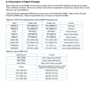
Most of the pins on the 970MP are the same as those found on the 970FX package, though the pin placement is different. However, there are a number of pins that are duplicated, one per core, several new or modified pins, and a few deletions. Table 8-2 lists the duplicated 970FX pins, one per core on the PowerPC 970MP.
 
The 970 has one pin I2CSEL Allows external selection of the I2C or JTAG interface for controlling scan functionality. I will check its location on the cpu.
 
After looking at the bottom of a G5 Logic board and I have noticed what could be JTAG points.

I am going to be examining the motherboard more closely, there appears to be four of these points and just beneath the cpu connector there is a row of test points. I was looking at photos on line when I noticed these. I need to look at my own equipment and sees if there is any indication on what these are for.

I will update you all soon as possible.
 
We could be a step closer to overclocking our G5's or to underclock them. This would make sense if everything is located on the Logic board rather than the cpu daughterboard.

Lets wait and see.
 
This is the G4 Logic board and you can see the JTAG at the bottom of the photo on the right of the electrolytic capacitors to the right of the small chip, the JTAG is labeled DEBUG. The pinouts are not listed.

My point is that the manufacturer was in the habit of actually putting it on the Logic Board.
 

Attachments

  • s-l1600.jpg
    s-l1600.jpg
    664.8 KB · Views: 94
Last edited:
Now I was reading on the Interweb more about JTAG and it should allow us to access the speed of the CPU, how long we can leave the CPU in test mode we do not know at the moment, It should also allow us to underclock the cpu and bus speed.

I will be starting to test for JTAG connections very soon. I need to acquire another G5 computer to experiment with as I really do not want to use my Quad.
 
  • Like
Reactions: PowerfulEra
I am going to have to open up my Quad's LCS and sort it out, there is no leak but it has been standing a while without being used so this is an excellent opportunity to start searching for JTAG. I will try to get round to posting photographs as I start.

I have read a lot of info on what other folk have done. In reality there is an awful lot of space to play with to experiment with the MP cooling. I have to remind myself if I manage to solve the overclocking I need something extraordinary to cool the cpu.
 
People want photos of evidence, the problem here is that we are dealing with possibilities and theory at the moment until proper testing is available to achieve. I have got to find the time next to start ripping my G5 apart to in order sort out problem with the LCS. This could take me a while due to other commitments so watch this thread.
 
I have just spent 10 minutes with with Quad trying to get it to work after it standing unused for 3 years, I have reseated the graphics card and replaced the ram and it now boots perfectly. I pressed the SMC reset button located on the logicboard at the bottom as well.

My Quad must be one of the few that has not leaked and is in great condition.

My dual 2.5 Powermac on the other hand has failed to boot, but I have not done a lot of tests yet.
 
Last edited:
  • Like
Reactions: pc297
So I am not going to take apart the Quad now it is back up and running but instead I will see what my Dual 2.5 does as this as also been in storage and not been used. It would be very odd if the LCS has clogged in this but not the Quad. Both machines have been standing right next to each other in the various locations where they have been stored and both have been wrapped in bubble wrap to prevent scratching. I will start and diagnose the problem with the dual 2.5 over the weekend.

What we do know is that the coolant in both Macs can with stand cpu's running at faster speeds.
 
I have just spent 10 minutes with with Quad trying to get it to work after it standing unused for 3 years, I have reseated the graphics card and replaced the ram and it now boots perfectly. I pressed the SMC reset button located on the logicboard at the bottom as well.

My Quad must be one of the few that has not leaked and is in great condition.

My dual 2.5 Powermac on the other hand has failed to boot, but I have not done a lot of tests yet.
Mine is also one of the later versions having Delphi rev2 pumps (from Jan 2006) and still hasn't clogged either :) I do run it every few days briefly to make sure that it doesn't !
 

Power tuning through frequency scaling • Software initiated slow down of the processor; selectable to a half or quarter of the nominal operating frequency • Programmable latency for power mode transitions to control current spikes

Could we test this for overclocking, it we can fine what in OSX controls the CPU clock speed.
 
Last edited:
Register on MacRumors! This sidebar will go away, and you'll see fewer ads.