
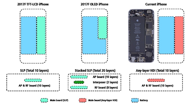
As the launch of Apple's iPhone X approaches tomorrow, eager users are set to enjoy battery life normally reserved for Apple's Plus-size form factors in a phone more closely resembling a non-Plus variant in its dimensions. The reason for this advancement is not an energy density development, but rather a smaller printed circuit board (PCB) inside the iPhone X, according to a February report from KGI Securities.
???????,??????? pic.twitter.com/7wzrBLVsFy - Anson Chen ? (@AnsonChen) November 2, 2017
This smaller PCB is thanks to a technology referred to as substrate-like PCBs, or SLP. Depictions from the report show a PCB with more layers than a traditional iPhone PCB thanks to application processor and RF signal-chain dedicated PCBs married via an interposer, creating a layer stackup nearly twice that of a conventional iPhone PCB.
However, this doesn't come close to telling the whole story. While a new PCB stackup may offer some more flexibility in component placement, it's important to remember that the opposite side of the board from the A11 isn't empty in an iPhone 8. There are plenty of components there too -- the NFC chip, display drivers, Wi-Fi combo chips, and power management ICs have all often found their homes directly opposite the workhorse application processor.
After all, 4.7-inch iPhones and their 5.5-inch "Plus" siblings have similarly sized PCBs, with battery capacity suffering as a direct result in the smaller phones. Herein lies the real problem in trying to improve battery life in these smaller form factors.
Click here to read rest of article...
Article Link: Prime Real Estate: The Fight for Space in the iPhone X

