The History of Apple SoCs
To know where we're going, we need to know where we came from. Prior to the A4, Apple sourced Samsung SoCs for the iPhone, iPhone 3G and iPhone 3GS. Let's take a look at Apple's custom SoCs.
A4
A4:
[10]
A5:
[9]
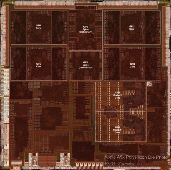
[8]
A6:
[7]
[6]
A7:

[8]
[11]
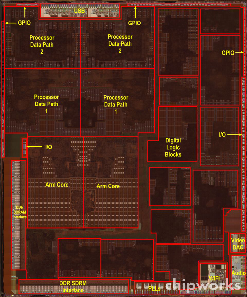
Functional block size allocation on die:
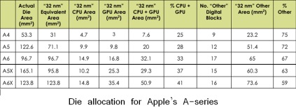
[12]
A8 Prediction
A8
A Look Back to Last Year
First of all, I should state this is not my first time doing this. I did an A7 prediction thread last year, which you can find linked in the more reading section. The prediction proved to be almost exactly on for the GPU, just narrowly missing on operating frequency but getting the configuration correct. It also correctly predicted the foundry and process, though that was not hard with the strength of the rumors suggesting Samsung's 28nm process. It also predicted the RAM type (LPDDR3) and size (1GB), but missed on frequency (1333 vs. 1600 MHz).
The post also accurately predicted the cellular radio and transceiver, though that prediction was largely piggy-backed on the work of Brian Klug from Anandtech. The WiFi chip was predicted to not change, and it did not. This came down to predicting whether Apple would adopt the AC standard with the new iPhone, which I predicted it would not due to their history of not adopting the latest in WiFi standards in their iOS devices.
The display was correctly predicted to not change based on the fact that Apple has never changed the display in successive phone generations (this is also true of form factor). I downplayed the idea of a phone with 128GB NAND storage, despite its technical possibility, because of what I perceived to be a combination of challenges involving number of SKUs, product ceiling, and market demand/tolerance of certain storage sizes. I also predicted a battery chemistry change prior to the release of the iPhone 5, which carried over to the 5S.
Where the prediction was wildly off the mark was the CPU. I had followed suit with Anandtech and Ars Technica in assuming that the CPU would be some modified version of Apple's custom core in the A6 SoC, codenamed "Swift." There were quite a few factors in that prediction. First, Swift was a fully custom core, which is very expensive, time-consuming, and rare in today's IC world. Many companies rely on automatic "place and route" tools that synthesize their logic into a layout automatically. By feeding the tools the constraints that will help them meet their target operating frequency, they can have the elements automatically placed much faster than a designer could hand-place them. This is at the expense of optimizing die area, speed, and power usage. Many other mobile SoC designers are able to rely on ARM's reference designs for their CPU cores as well, using the design as-is and tailoring other components around it. The only other prominent names for the consumer space that do custom designs is a short list: Intel, AMD, Qualcomm. Nvidia joins that list with their project Denver, which is a curious case that will be discussed later.
Swift being a custom design meant that the time to design it was lengthened, likely a process that took over the one year cadence that the iPhone design release cycle demanded. This made it likely that they would iterate on this design in small but meaningful ways given what I expected to be their limited manpower. For Swift's successor to be custom as well would likely mean that both designs were in active work simultaneously, necessitating a sizable work force. Finally, it had not been that long since ARM had announced the ARMv8-A ISA and A57 reference design. ARM made the first disclosure of its 64 bit architecture in October of 2011. It was a full year later before they announced their high-end 64 bit reference design, the A57. That meant that Apple had less than a year after the reference design was announced to get their own custom solution to market. Previously, the quickest time to market had been the previous generation, where Cortex A15 designs took about 2 years from the September 2010 licensing availability date to get their own designs out, and that was a comparatively simple iteration on an established ARMv7 ISA. It seems extremely likely that Apple began the design of the Cyclone clone shortly following ARM's disclosure of the ARMv8-A ISA, and they likely had an architecture concept even before then.
It is easy to see the factors working against a custom 64 bit CPU core designed by Apple, despite the rumors, but that is exactly what they did. At the time of this post, there is still no competing mobile device available on the market with a ARMv8-A compatible CPU core. This looks to likely be the case into 2015. Qualcomm, who is rushing their own design, is basing the Snapdragon 808 and 810 on the A57 reference design rather than doing a custom solution, as they have done with the rest of the Snapdragon series. The technically-inclined blogosphere was stunned by this announcement, and an unnamed Qualcomm employee called it a punch to the gut.
This is all in addition to the design providing yet another 2x benchmark improvement, boasting a very wide execution core, and having an impressive transistor density that was approximately double its Swift predecessor. It is truly an impressive undertaking and the chief reason I will never underestimate Apple again when it comes to aggressive time-to-market strategies.
The next biggest miss was the prediction of two distinct SoCs - one for the iPhone, iPad mini and iPod touch line of devices and one for the full-sized iPad line. This was based on the existence of the A5X and A6X SoCs which featured GPUs approximately double in performance to that of their non-"X" designated siblings. They also featured memory interfaces that were double in size, necessary to feed the larger GPUs, and large display resolution of the full-sized iPads. Instead, Apple went with the single A7 SoC offering and a GPU that actually performed below its predecessors in some benchmarks. They did manage to compensate for the memory bus width decrease by moving to much faster 1600 MHz LPDDR3 RAM, however. It seems apparent that Apple is now satisfied with memory bandwidth and GPU performance of the standard iPhone-level SoCs for iPad use and will go with a single SoC strategy moving forward where it only differentiates on the clock speeds and packaging. Packaging may need to be unified such that the RAM is no longer off package as seen in the full-sized iPads in the future, however, as is discussed a bit later.
What I feel the takeaway should be from this is that despite Apple's secretive nature regarding product roadmap, it is possible to predict the components used in their future devices simply based on analyzing their product history. By noting their revision cycle, tendencies on adopting new protocols, current or near-term technology advancement and availability, and their reactiveness to the market (or lack thereof), we can get a somewhat accurate glimpse of where their products may be headed.
SoC
These predictions are based on a mixture of supply chain rumors, historical cadence in Apple's SoC offerings and inference based on what parts are available on the market that would make sense for Apple's likely goals.
CPU
Comments on Cyclone
Before we begin this year's CPU core prediction, let's try to understand what type of evolution that Cyclone was to Swift. Last year, I predicted an evolution of Swift for the CPU core, with things like L2 pre-fetch and better branch prediction evolving the Swift core. I compared Swift to Qualcomm's Krait architecture because of their similarities in clock speeds and pipeline depths. In that context, I suggested that improvements that been made to the Krait architecture would find their way into the Apple design as well. Krait's pre-fetchers are quite a bit better than the standard ARM ones, making that one area I suggested Apple could perhaps be making improvements.
Cyclone turned out to be a major change from Swift. Shown below is a table from Anandtech's detailing of the Cyclone architecture and comparing it with Swift. Since Apple does not publicly disclose architecture details, the information has to be gleaned from LLVM commits. That microarchitecture piece contains more than is discussed here, and is highly recommended reading.

[16]
Other than the ISA change, the first thing that jumps out about the change is that Apple doubled the issue width. This means that the Cyclone core can dispatch twice as many instructions as Swift at a time. With their identical clock frequencies, it's easy to see where their claimed 2x speedup came from. It also highlights the reason that they didn't go quad-core. Going with a wider core gives you more execution power without the overhead of adding circuitry for an independent core capable of running separate threads. However, the issue with dispatching so many instructions at once is data dependencies. If one instruction depends on the outcome of another, that instruction will stall until its required data is ready, slowing the processor down. That leads us to the re-order buffer. It is over four times as large as Swift, which means it can shift instruction execution order around such that these data dependencies never manifest in the actual execution order.
We can see that the branch mispredict penalty is slightly increased. This is likely a byproduct of a more complex core with more concurrent execution possibilities and potentially a deeper pipeline. What this means is that when you reach a conditional instruction that depends on a variable that is determined at runtime, you have to assume some outcome of that conditional instruction so that you can execute instructions that come after it without waiting for its result. In the event that your architecture guesses wrong, you must flush the pipeline and discard all instruction results that depended on that being the correct prediction. The techniques to mitigate misprediction are beyond the scope of this piece, but it suffices to say it's an important part of the architecture that has a significant contribution to overall performance. Furthermore, in addition to doubling the branch units, we can see they've also added an indirect branch unit. This is a type of branch where the destination address is not immediately known, such as being stored in another memory address. Given that this address may not necessarily be loaded into cache, it may take a while to retrieve this data, so having a unit to address this possibility can also cut down on wasted CPU cycles.
The load/store units and ALUs have also essentially been doubled, which makes sense with double the issue width. General purpose and floating point registers doubled as well, as is called for by the ARMv8 ISA. L1 Instruction and data cache have also been doubled. The reason for this relates to memory hierarchy. Modern CPUs often have 2 to 3 levels of cache. With each successive level, the size increases, as does the associativity and access latency. Thus, a processor with double the issue width simply can't rely on a large L2 to feed it data quickly when the latency is much longer than the L1. Associativity and eviction type are reasons why the L1 cache is separated into instruction and data caches.
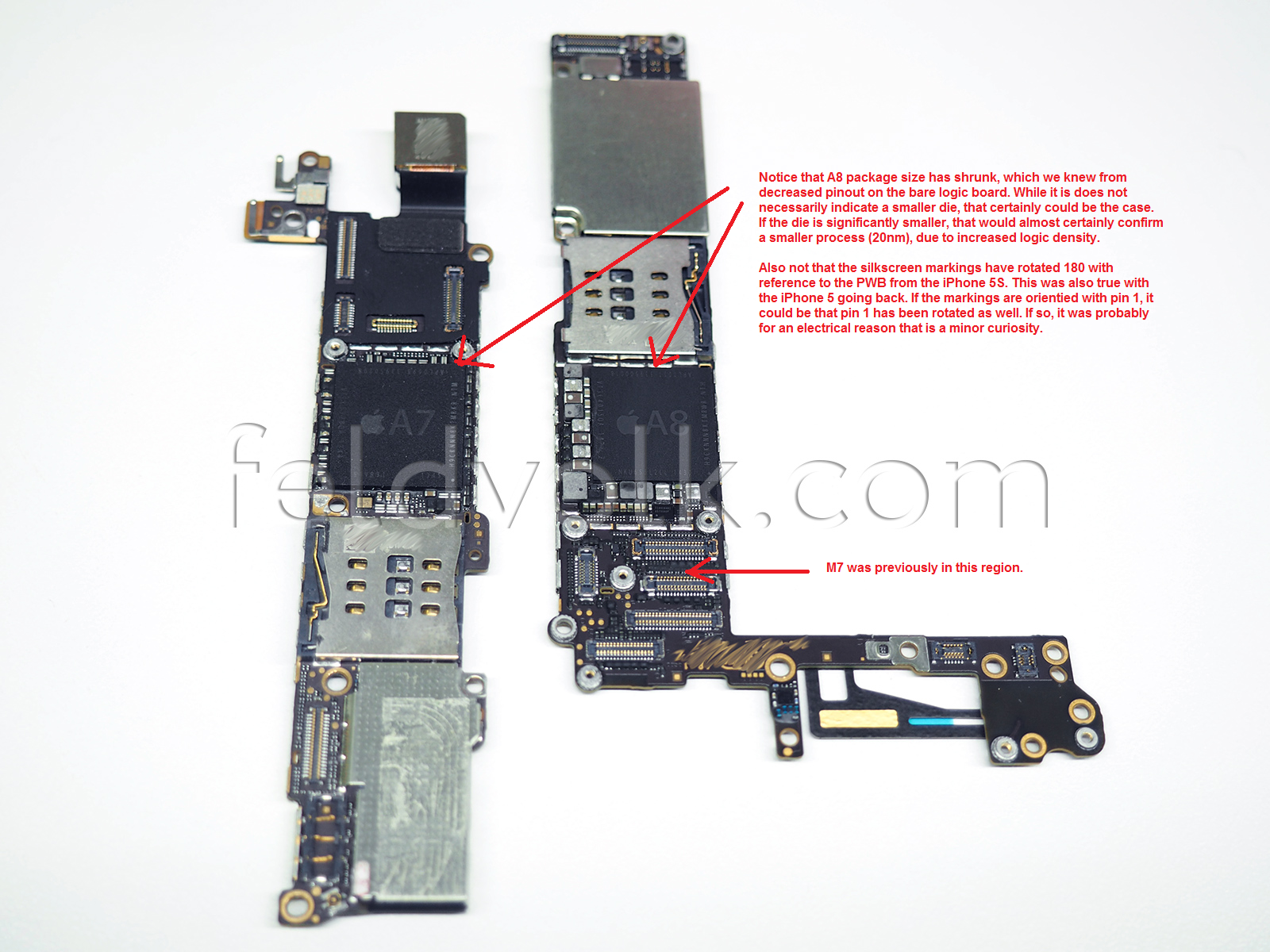
Finally, Apple decided to add an L3 cache of 4MB. We know from the Anandtech review of the Retina iPad mini that this cache services the CPU, GPU, and the Image Signal Processor (ISP). In addition to extra cache space for the CPU which cuts down on average total memory access latency. It is also significant that the GPU and ISP can access it, given Apple's new camera software enhancements call for a lot of real-time image processing. It could also improve GPU performance, though that would depend on how programmable it is for the end-user developer. If the cache did have some programmability, it could act as a mitigating factor for main memory bandwidth drop from the A6X to A7 for the full-sized iPad, similar to the eDRAM in the Xbox 360 and the eSRAM in the Xbox One consoles. However, I've not seen anything to indicate that this it the case. The result of doubling all of these execution units and adding a large L3 cache was that the transistor count roughly doubled to over 1 billion, as reported directly by apple in the keynote. This is significant because the die area actually decreased from A6 to A7. That is in large part owing to the fact that the L3 cache is 4MB, which is approximately 196 million transistors alone.
For reference, TSMC also claims a 1.9x transistor density increase going from their 28nm to 20nm process, all other things constant. However, in this case, the design changed completely, negating one of those factors. Also, the transition from 28nm to 20nm is actually what is known a full-node transition. The change from 32nm to 28nm, as we saw in A6 to A7, is a half-node transition. Half-node transitions tend to be simple optical shrinks of the prior generation with mostly the same tooling and processes, whereas full-node transitions require all-new tooling and constitute much larger financial investments by fab houses. All of this taken into account, it is very impressive that Apple achieved this transistor density increase on a half-node transition, despite the large, dense L3 cache helping them reach that mark. It is truly a testament to the expertise of their custom design personnel, who improved significantly on an already custom A6 design.
The A8 CPU prediction
When talking about Apple's CPU efforts, it's important to remember how they got the capability level they are at now. Acquiring Intrinsity, PA Semi, among others, and hiring top CPU architects from AMD shows how serious Apple is about top performing, custom CPU solutions. Apple also turned heads with their Macroscalar trademark two years ago, but it is unclear whether any technology related to this has come to market or why Apple felt the need to trademark what would likely be considered a trade secret design process. Moreover, all speculation about the trademark seems to come back to established methods of branch prediction and speculative execution. It will be interesting to see if this topic comes up again at all.
Cyclone and Swift were each sweeping achievements over their successors, and the circumstances make it very tough for Apple to repeat the leap forward once again. Accordingly, the CPU prediction is rather mild this time around. The move to 20nm from 28nm will certainly help in terms of transistor density and speed for the same amount of power, but Apple's history of extremely modest clock speeds suggests we'll see little movement on this front again. For the iPhone, Cyclone stayed at the same 1.3 GHz that Swift was rated at, despite top end Android handsets boasting quad-core architectures with max CPU speeds above 2 GHz. The reason for restraint on clock speed is to save power, but it helps to know exactly how this saves power.
The power of a transistor operating in a digital function is expressed with the equation P = fCV^2, where f is the frequency of operation, C is the capacitive load of the element that the transistor is driving, and V is the voltage applied to the drain of the transistor that it switches back and forth to from ground. It becomes clear that the dominant factor is likely going to be voltage, as power goes up with its square. What's not clear is that the frequency at which you can operate is directly tied to the voltage you operate at because it directly determines how fast you can move electrons to switch states. Thus, by picking a modest frequency to operate at, you can likely pick a voltage that is lower than your competitors who choose to clock their CPUs at or above 2 GHz. To get a similar amount of performance, you simply compensate by adding bigger or more cores. Apple's reluctance to add more cores means they have opted for wider cores. They now sit alone atop of the heap of mobile CPU designers in core width. In fact, as Anand points out in his Cyclone overview, it's as wide as desktop designs such as Sandy Bridge. That definitely warrants the term "desktop class" Apple proudly boasted in the last keynote.
Apple's crown of core width is set to expire next year, however, as Nvidia will introduce their own 64-bit ARMv8-A compatible core with an issue width of 7. That core is a fair bit more complex, however, as it is not a native ARMv8-A core and will rely on binary translation to interpret ARMv8-A machine code. I definitely suggest the preview if this concept interests you more. However, this, along with Qualcomm's own plans to adopt dual-core A57s, should show that large, complex cores in a dual-core configuration is the most optimized solution for mobile at the moment. The "core-war" started by Nvidia's quad-core Tegra 2 seems to finally be subsiding. I have no doubt that mobile environments will benefit from four cores, whether logical or physical, sometime in the future, but it does seem to be later rather than sooner at this point.
Apple has also been in a perfect storm of ISA advancements, reference core designs, and shorter times-to-market for designs. Apple first moved to the Cortex A8 architecture and associated ARMv7 ISA with the iPhone 3GS, two years after the reference design had been disclosed. The Cortex A8 had significantly higher IPC than its ARM 11 predecessor that implemented the ARMv6 ISA. The following year, they used another Cortex A8 design, this time customized by Intrinsity and clocked 50% faster. That was Apple's first custom SoC, dubbed the A4. The Cortex A9 followed, boasting an out-of-order design for another hefty IPC boost. Apple placed two of these cores in their A5 SoC while holding clock speeds steady. Cortex A15 followed with some ISA extensions that put us up to ARMv7s, codenamed "Eagle", which Apple departed from in their first truly custom design codenamed "Swift" in the A6. Another clock boost around 50% allowed them to achieve another 2x benchmark improvement over the A5 design. Most recently, Apple took advantage of another ISA announcement, ARMv8-A, to create their "Cyclone" core in the A7. This design was able to achieve its 2x improvement via a big IPC improvement and more powerful instructions at their disposal while holding the CPU frequency constant. Given this cadence, it seems reasonable to expect some CPU frequency increase this time around.
Now, Apple finally sits at a juncture where there is no new ISA to implement, no new reference core to modify, and no clear low-hanging fruit in terms of design improvements to significantly upgrade over their predecessor. Issue width seems unlikely to increase, given the design is already as wide as many desktop designs. Further attempts to widen the core would likely result in underutilized functional units with little boost to overall actual IPC. Considering all of these factors, it will be quite tough for Apple to achieve a third consecutive 2x benchmark improvement claim unless they significantly increase clock speeds. I feel that it is much more likely that Apple will make small but meaningful improvements to the existing Cyclone design, potentially addressing what they feel are its biggest shortcomings. Examples of what this might include are a better branch predictor, more custom extensions to the ARMv8-A ISA to speed-up frequently used operations, memory latency time reductions, or reductions of cycles needed for complex ALU operations.
In last year's piece, I also spent some time explaining the drawbacks of a quad-core design or implementing ARM's big.LITTLE heterogeneous core topology scheme, and those points are still relevant moving forward. More of this design trade is explained below in the section on TDP, die size, and other design considerations.
GPU
All versions of the iPhone have featured a GPU from Imagination Technologies. In fact, Apple owns around a 10% stake in them as well (an interesting side note- ImgTec acquired Caustic Graphics, a company focused on creating dedicated ray tracing hardware that was comprised of former Apple engineers). It seems all but certain that Apple's A8 will feature ImgTec graphics core as well, with Imagination Technologies announcing a multi-year, multi-use extension to their licensing agreement with Apple. Last year, ImgTec's Series 6 "Rogue" architecture was brand new with many performance improvement claims, so it was a big area of interest as a potential upgrade. This year, however, we only have a modest update to that series to eye as a potential upgrade.
One positive thing about the GPU landscape is that ImgTec has been very good about publishing data on their architectures over the course of the past year. This includes a very good comprehensive overview of the Series 6 family of GPUs and a good article on the specific improvements that the 6XT line of GPUs offers over the initial Series 6 GPUs. You can read the articles to get a detailed explanation of the improvements, but they boil down to better DVFS, better compression techniques, higher FP16 performance and improved scheduling. FP16 performance has historically been the determining factor in mobile graphics environments, rather than the FP32 commonplace in the desktop graphics market. They claim performance boosts can be had up to 50%, though it is likely those are highly situation specific and real world improvements which be much more modest.
As to whether Apple intends to adopt the new 6XT series, it is largely a question of time to market. ImgTec has only recently introduced this line of GPUs at CES in January. Given this would represent a time table that is very aggressive and much faster than any other GPU (or CPU) architecture adoption, it seems rather unlikely. ImgTec originally made Series 6 cores available for licensing in January of 2010. It followed that 6 months later with the G6x30 series, that were focused on performance rather than area and featured additional compression technology in addition to more FP16 ALUs. That meant the G6430 in the 5S had a 14 month time to market from being announced. The timetable would only be 9 months if Apple chose to use the G6450 or G6650 GPUs.
However, Apple has many things working in their favor when it comes to adoption of a potential G6x50 GPU solution. Given that they are a 10% stakeholder and the most significant party when it comes to licensing revenue, it is likely they would have early access if they sought it. The GPU architecture's similarity to its predecessor likely means it is also easier to iterate than it would have been to go from the series 5 to series 6 GPUs. The architecture also has many improvements to refine its power consumption, and some of the DVFS improvements in particular were added in response to customer feedback. It seems likely that Apple would have been one of the parties providing such feedback.
Last year, I also addressed Apple's GPU engineer team in Orlando, FL. I suggested it could indicate that they intended to create their own customized versions of ImgTec GPUs, fully custom GPUs, or API/driver improvements to speed things up from the software side. Apple confirmed my last suggestion when they announced the "Metal" (a reference to "coding to the metal", or low level programming that directly addresses the features of the hardware) shader programming language designed to eliminate driver overhead when writing graphics code. Driver overhead can be significant, as well. It is the reason that AMD introduced their own custom graphics API, Mantle. It's also the reason that video game consoles are able to succeed in the face of much more powerful PCs. It is quite possible that my other ideas on this team's function may come to fruition, but this advancement could potentially allow for graphics tasks to run faster than before even if Apple does nothing to update the GPU. In this sense, they could get a free GPU update and may not feel it is necessary to touch the GPU architecture for A8.
In light of these facts, I still think it is highly likely Apple decides to increase the size of the GPU by going to a 6 cluster configuration in addition to or instead of adopting the new G6x50 architecture improvements. They will likely benefit from a full node transition by going to 20nm and the CPU cores seem unlikely to grow significantly, affording plenty of die space to increase the performance of the GPU. This will be especially important if this year's product cycles introduces any more demanding resolutions among their iDevice offerings. From a prediction standpoint, it is exciting to think about the possibility of a G6x50 GPU offering because it represents an aggressive time to market benchmark new for even Apple.
It is worth noting that ImgTec has also introduced a variant of the 6 Series GPU that features dedicated ray tracing hardware. Ray tracing is a physically based lighting method that is more accurate than traditional rasterization methods but much more computationally expensive and memory intensive. CPUs and even GPUs do not do it well. There have been previous attempts to do it with custom silicon that have also failed. However, ImgTec recently acquired Caustic Graphics who have dedicated hardware solutions, which according to famous graphics programmer John Carmack, are actually quite good. ImgTec decided to integrate it into their Series 6 GPUs, making them the first consumer GPUs with dedicated ray tracing hardware.
The problem with ray tracing hardware is that developers would have to implement support for it to actually be useful. While some applications that render 3D graphics may be able to make use of it, the primary use would likely be games. It is often a tough sell to get developers to put major features into games that only a small subset of users will utilize. This is above and beyond the technical challenges it poses. Indeed, before being disclosed on the Caustic hardware, Carmack stated with 90% certainty that any eventual ray tracing hardware would likely be small modifications to existing GPUs. He also downplayed the need for it all together in modern games. Thus, it is likely to be relegated to a curiosity for at least the next few years. The future does have promise though, as ImgTec has already acknowledged the existence of the 7 Series family of GPUs, along with indications that they plan to iterate designs at a faster pace in the future. It seems very likely that we will be talking about the 7 Series much more in the near future, possibly as a GPU candidate for the next wave of GPUs utilized in custom Apple SoCs.
RAM
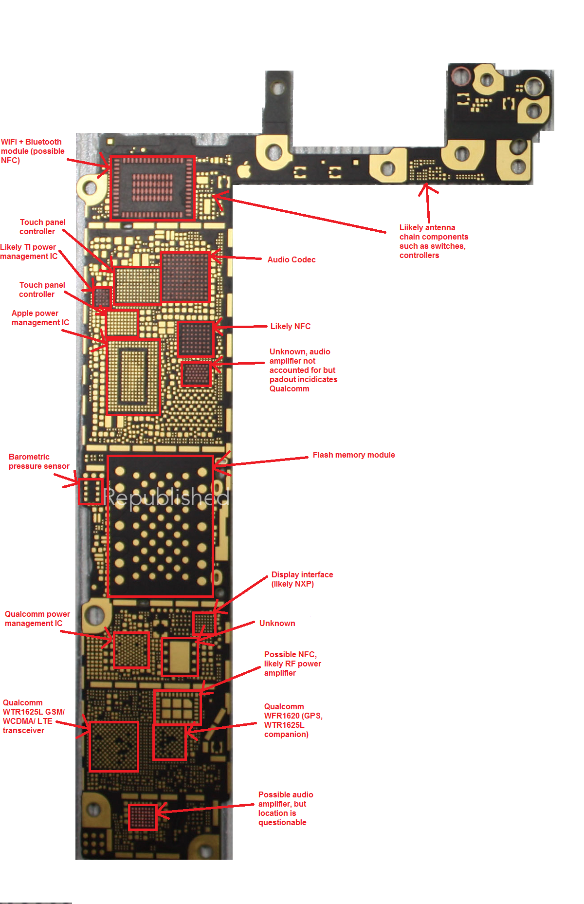
It seems as though this one may have already been determined, based on the populated PCB leaks recently. Using the Hynix mobile memory code reference sheet, it has been determined that the A8 likely has 1GB of 1600 MHz LPDDR3 RAM, the same as its predecessor, with what is assumed to be a 64-bit data bus. The fact that it suggests A8 only has 1GB of RAM is particularly surprising, because as you can see from the list of previous iPhones, Apple has never kept the same amount of RAM in the iPhone for more than 2 generations. Many aspects of their devices have a 2 year cadence including but not limited to form factor, product naming, screen size and technology, and many other features. This also comes into contrast with a rumor earlier this year that suggested Apple may look to include the new LPDDR4 RAM in their iDevices this year. Part of the rumor was based on a 250 million dollar mystery payment made to Micron (who now own Elpida, memory supplier on previous iPhones). While Apple has been known to make large payments to suppliers in the past in order to secure volume and favorable pricing, it seems that this supposition was perhaps unfounded in this case. A large part of the reason it likely cannot be adopted is because suppliers cannot provide volume or acceptable pricing for Apple's needs. Indeed, the standard for LPDDR4 was just ratified by JEDEC in the past week. That being said, LPDDR4 is a significant improvement over LPDDR3, much more so than LPDDR3 was over LPDDR2. It has a lower voltage and completely new interface that will offer significantly more speed and power savings. Apple will likely look to adopt it as soon as possible given their volume and pricing constraints.
In an effort to be critical of what we assume is known about the RAM in the A8 processor, I will offer possible thoughts to suggest our assumed knowledge may not be correct. First, there are several unknown letters in the memory sequence, as is discussed in the linked thread, that suggest a few unknowns may exist. Since the code does not clearly indicate bus-width like Elpida part numbers have in the past, it is possible we may be looking at a data bus wider than 64 bits. Apple has used 128-bit data buses in their A5X and A6X processors in the past. The bus width was needed to drive the large number of pixels in the iPad retina displays, and the memory chips were located off package for thermal reasons, in addition to the difficulty of having a wide memory bus such as that in a PoP memory configuration.
Interestingly, Chipworks' analysis of the A7 revealed that the memory package had decreased their pad pitch and increased the number of pads from 272 in the A6 to 456 in the A7. This further explains the memory code not being listed and gives us a clue as to what may be changing between the A7 and A8. Given that the LPDDR3 standard doesn't call for extra pins over the LPDDR2, they correctly questioned what the large pad increase was if the bus width remained at 64-bit. While this question was never answered, it does point to the possibility that Apple has the capability to properly package memory with the processor and achieve a bus width of 128 bits. It also may indicate that in the misunderstanding of the part number, such that there are two such dies of 1GB each, that add to a total of 2GB.
It is also possible that with the introduction of a 5.5" iPhone model, Apple may seek to differentiate them further by offering them with differing RAM amounts, among other features. Apple has not given their iDevice line different RAM amounts for the same processor since the iPhone 4 had 512 MB compared to the original iPad's 256 MB, however. It is also interesting that Apple continues to put the RAM off package in the full size iPad while clocking it only modestly higher when the iPhone and iPad mini with Retina clearly show that the A7's heat output can be handled in small form factors without aggressive thermal management techniques. I expect Apple to eventually stop doing this for the RAM in the iPad Air, especially since future 3D IC technologies will demand it.
Looking into the future, it is likely that we will eventually see 3D IC memory solutions from Apple for their SoCs. Rather than having individual solder bumps from the memory chip to the interconnects, 3D IC solutions allow the memory to directly interconnect to the SoC through a silicon substrate by what are called through silicon vias (TSV). This will allow for greatly expanded memory interfaces that are 512 or even 1024 bits wide in comparison to the 64 and 128 bit interfaces currently seen in the iPhone and iPad. Sony uses a predecessor to this technique called System in Package (SiP) that uses fine wires as opposed to solder bumps, allowing them to achieve more interconnects in a given space. This allows the Vita's GPU to have a 512 bit interface to its VRAM. Whatever solution they use, it will allow Apple to greatly improve memory bandwidth, which can bottleneck GPU performance.
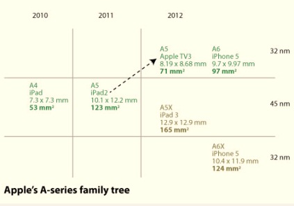
To know where we're going, we need to know where we came from. Prior to the A4, Apple sourced Samsung SoCs for the iPhone, iPhone 3G and iPhone 3GS. Let's take a look at Apple's custom SoCs.
A4
A4:
[10]
- Manufacturer - Samsung on 45nm process (as featured in iPhone 4)
- Die Size - 53 mm2 [5]
- Designer - Apple (Intrinsity[3], also featured in Samsung's 'Hummingbird' SoC[4])
- CPU Type - 800MHz Cortex-A8 Core with Intrinsity customizations
- Core Count - 1
- Instruction Set - ARMv7
- Chip Designator - S5L8930X
- L1 Cache - 32/32KB (Instruction/Data)
- L2 Cache - 512KB
- RAM - 512MB LPDDR @ 400 MHz (as seen in iPhone 4, 64 bit interface, PoP)
- Max Theoretical Memory Bandwidth - 3.2 GB/s [1]
- GPU Type - Dual Core PowerVR SGX 535 @ 200 MHz
- GPU Performance - 1.6 GFlops, 14 MTriangles/s [2]
A5:
[9]
- Manufacturer - Samsung on 45nm process (as featured in iPhone 4S)
- Die Size - 122.2 mm2
- Designer - Apple
- CPU Type - 800MHz Cortex-A9 Core with customizations
- Core Count - 2
- Chip Designator - S5L8940X
- L1 Cache - 32/32KB (Instruction/Data)
- L2 Cache - 1MB
- RAM - 512MB LPDDR2 @ 800 MHz (64 bit interface, PoP)
- Max Theoretical Memory Bandwidth - 6.4 GB/s [1]
- GPU Type - Dual Core PowerVR SGX 543 @ 200 MHz
- GPU Performance - 14.4 GFlops, 70 MTriangles/s [2]
[8]
- Manufacturer - Samsung on 45nm process (as featured in 3rd generation iPad)
- Die Size - 165 mm2
- Designer - Apple
- CPU Type - 1GHz Cortex-A9 Core with customizations
- Core Count - 2
- Instruction Set - ARMv7
- Chip Designator - S5L8945X
- L1 Cache - 32/32KB (Instruction/Data)
- L2 Cache - 1MB
- RAM - 512GB LPDDR2 @ 800 MHz (128 bit interface, off package)
- Max Theoretical Memory Bandwidth - 12.8 GB/s [1]
- GPU Type - Quad Core PowerVR SGX 543 @ 250 MHz
- GPU Performance - 36 GFlops, 175 MTriangles/s [2]
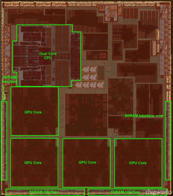
A6:
[7]
- Manufacturer - Samsung on HKMG 32nm process
- Die Size - 96.71 mm2
- Designer - Apple
- CPU Type - 1.3GHz "Swift" Core
- Core Count - 2
- Instruction Set - ARMv7s
- Chip Designator - S5L8950X
- L1 Cache - 32/32KB (Instruction/Data)
- L2 Cache - 1MB
- RAM - 1GB LPDDR2 @ 1066 MHz (64 bit interface, PoP)
- Max Theoretical Memory Bandwidth - 8.5 GB/s [1]
- GPU Type - Triple Core PowerVR SGX 543 @ 333 MHz
- GPU Performance - 36 GFlops, 175 MTriangles/s [2]
[6]
- Manufacturer - Samsung on HKMG 32nm process
- Die Size - 123 mm2
- Designer - Apple
- CPU Type - 1.4GHz "Swift" Core
- Core Count - 2
- Instruction Set - ARMv7s
- Chip Designator - S5L8955X
- L1 Cache - 32/32KB (Instruction/Data)
- L2 Cache - 1MB
- RAM - 1GB LPDDR2 @ 1066 MHz (128 bit interface, off package)
- Max Theoretical Memory Bandwidth - 17 GB/s [1]
- GPU Type - Quad Core PowerVR SGX 554 @ 280 MHz
- GPU Performance - 71.7 GFlops, 210 MTriangles/s [2]
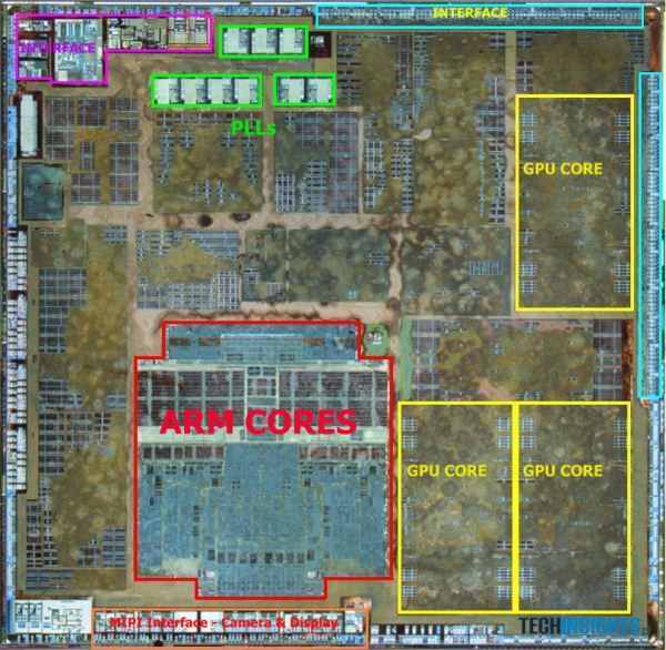
A7:
[8]
- Manufacturer - Samsung on HKMG 28nm process
- Die Size - 102 mm2
- Transistors - Approximately 1 billion
- Designer - Apple
- CPU Type - 1.3GHz "Cyclone" 64-bit Core (1.4GHz for iPad products)
- Core Count - 2
- Instruction Set - ARMv8-A (with custom Apple extensions)
- Chip Designator - S5L8960X
- L1 Cache - 64/64KB (Instruction/Data)
- L2 Cache - 1MB
- L3 Cache - 4MB
- RAM - 1GB LPDDR3 @ 1600 MHz (64 bit interface, PoP for iPhone)[13][14]
- Max Theoretical Memory Bandwidth - 12.8 GB/s
- GPU Type - "Quad Cluster" PowerVR 6430 @ 450 MHz[15]
- GPU Performance - 115.2/172.8 GFlops (FP32/FP16)
[11]
Functional block size allocation on die:
[12]
A8 Prediction
A8
- Manufacturer - TSMC on HKMG 20nm process
- Die Size - 100-120 mm2
- Designer - Apple
- CPU Type - 1.5GHz Third Generation Custom Apple Core
- Core Count - 2
- Instruction Set - ARMv8-A (with custom Apple extensions)
- Chip Designator - S5L8970X
- L1 Cache - 64/64KB
- L2 Cache - 1MB
- L3 Cache - 4MB
- RAM - 2GB LPDDR3 @ 1600 MHz (64 bit interface, PoP for iPhone)
- Max Theoretical Memory Bandwidth - 12.8 GB/s
- GPU Type - "Hex Cluster" PowerVR GX6650 @ 450 MHz
- GPU Performance - 172.8/354.6 GFlops (FP32/FP16)
A Look Back to Last Year
First of all, I should state this is not my first time doing this. I did an A7 prediction thread last year, which you can find linked in the more reading section. The prediction proved to be almost exactly on for the GPU, just narrowly missing on operating frequency but getting the configuration correct. It also correctly predicted the foundry and process, though that was not hard with the strength of the rumors suggesting Samsung's 28nm process. It also predicted the RAM type (LPDDR3) and size (1GB), but missed on frequency (1333 vs. 1600 MHz).
The post also accurately predicted the cellular radio and transceiver, though that prediction was largely piggy-backed on the work of Brian Klug from Anandtech. The WiFi chip was predicted to not change, and it did not. This came down to predicting whether Apple would adopt the AC standard with the new iPhone, which I predicted it would not due to their history of not adopting the latest in WiFi standards in their iOS devices.
The display was correctly predicted to not change based on the fact that Apple has never changed the display in successive phone generations (this is also true of form factor). I downplayed the idea of a phone with 128GB NAND storage, despite its technical possibility, because of what I perceived to be a combination of challenges involving number of SKUs, product ceiling, and market demand/tolerance of certain storage sizes. I also predicted a battery chemistry change prior to the release of the iPhone 5, which carried over to the 5S.
Where the prediction was wildly off the mark was the CPU. I had followed suit with Anandtech and Ars Technica in assuming that the CPU would be some modified version of Apple's custom core in the A6 SoC, codenamed "Swift." There were quite a few factors in that prediction. First, Swift was a fully custom core, which is very expensive, time-consuming, and rare in today's IC world. Many companies rely on automatic "place and route" tools that synthesize their logic into a layout automatically. By feeding the tools the constraints that will help them meet their target operating frequency, they can have the elements automatically placed much faster than a designer could hand-place them. This is at the expense of optimizing die area, speed, and power usage. Many other mobile SoC designers are able to rely on ARM's reference designs for their CPU cores as well, using the design as-is and tailoring other components around it. The only other prominent names for the consumer space that do custom designs is a short list: Intel, AMD, Qualcomm. Nvidia joins that list with their project Denver, which is a curious case that will be discussed later.
Swift being a custom design meant that the time to design it was lengthened, likely a process that took over the one year cadence that the iPhone design release cycle demanded. This made it likely that they would iterate on this design in small but meaningful ways given what I expected to be their limited manpower. For Swift's successor to be custom as well would likely mean that both designs were in active work simultaneously, necessitating a sizable work force. Finally, it had not been that long since ARM had announced the ARMv8-A ISA and A57 reference design. ARM made the first disclosure of its 64 bit architecture in October of 2011. It was a full year later before they announced their high-end 64 bit reference design, the A57. That meant that Apple had less than a year after the reference design was announced to get their own custom solution to market. Previously, the quickest time to market had been the previous generation, where Cortex A15 designs took about 2 years from the September 2010 licensing availability date to get their own designs out, and that was a comparatively simple iteration on an established ARMv7 ISA. It seems extremely likely that Apple began the design of the Cyclone clone shortly following ARM's disclosure of the ARMv8-A ISA, and they likely had an architecture concept even before then.
It is easy to see the factors working against a custom 64 bit CPU core designed by Apple, despite the rumors, but that is exactly what they did. At the time of this post, there is still no competing mobile device available on the market with a ARMv8-A compatible CPU core. This looks to likely be the case into 2015. Qualcomm, who is rushing their own design, is basing the Snapdragon 808 and 810 on the A57 reference design rather than doing a custom solution, as they have done with the rest of the Snapdragon series. The technically-inclined blogosphere was stunned by this announcement, and an unnamed Qualcomm employee called it a punch to the gut.
This is all in addition to the design providing yet another 2x benchmark improvement, boasting a very wide execution core, and having an impressive transistor density that was approximately double its Swift predecessor. It is truly an impressive undertaking and the chief reason I will never underestimate Apple again when it comes to aggressive time-to-market strategies.
The next biggest miss was the prediction of two distinct SoCs - one for the iPhone, iPad mini and iPod touch line of devices and one for the full-sized iPad line. This was based on the existence of the A5X and A6X SoCs which featured GPUs approximately double in performance to that of their non-"X" designated siblings. They also featured memory interfaces that were double in size, necessary to feed the larger GPUs, and large display resolution of the full-sized iPads. Instead, Apple went with the single A7 SoC offering and a GPU that actually performed below its predecessors in some benchmarks. They did manage to compensate for the memory bus width decrease by moving to much faster 1600 MHz LPDDR3 RAM, however. It seems apparent that Apple is now satisfied with memory bandwidth and GPU performance of the standard iPhone-level SoCs for iPad use and will go with a single SoC strategy moving forward where it only differentiates on the clock speeds and packaging. Packaging may need to be unified such that the RAM is no longer off package as seen in the full-sized iPads in the future, however, as is discussed a bit later.
What I feel the takeaway should be from this is that despite Apple's secretive nature regarding product roadmap, it is possible to predict the components used in their future devices simply based on analyzing their product history. By noting their revision cycle, tendencies on adopting new protocols, current or near-term technology advancement and availability, and their reactiveness to the market (or lack thereof), we can get a somewhat accurate glimpse of where their products may be headed.
SoC
These predictions are based on a mixture of supply chain rumors, historical cadence in Apple's SoC offerings and inference based on what parts are available on the market that would make sense for Apple's likely goals.
CPU
Comments on Cyclone
Before we begin this year's CPU core prediction, let's try to understand what type of evolution that Cyclone was to Swift. Last year, I predicted an evolution of Swift for the CPU core, with things like L2 pre-fetch and better branch prediction evolving the Swift core. I compared Swift to Qualcomm's Krait architecture because of their similarities in clock speeds and pipeline depths. In that context, I suggested that improvements that been made to the Krait architecture would find their way into the Apple design as well. Krait's pre-fetchers are quite a bit better than the standard ARM ones, making that one area I suggested Apple could perhaps be making improvements.
Cyclone turned out to be a major change from Swift. Shown below is a table from Anandtech's detailing of the Cyclone architecture and comparing it with Swift. Since Apple does not publicly disclose architecture details, the information has to be gleaned from LLVM commits. That microarchitecture piece contains more than is discussed here, and is highly recommended reading.
[16]
Other than the ISA change, the first thing that jumps out about the change is that Apple doubled the issue width. This means that the Cyclone core can dispatch twice as many instructions as Swift at a time. With their identical clock frequencies, it's easy to see where their claimed 2x speedup came from. It also highlights the reason that they didn't go quad-core. Going with a wider core gives you more execution power without the overhead of adding circuitry for an independent core capable of running separate threads. However, the issue with dispatching so many instructions at once is data dependencies. If one instruction depends on the outcome of another, that instruction will stall until its required data is ready, slowing the processor down. That leads us to the re-order buffer. It is over four times as large as Swift, which means it can shift instruction execution order around such that these data dependencies never manifest in the actual execution order.
We can see that the branch mispredict penalty is slightly increased. This is likely a byproduct of a more complex core with more concurrent execution possibilities and potentially a deeper pipeline. What this means is that when you reach a conditional instruction that depends on a variable that is determined at runtime, you have to assume some outcome of that conditional instruction so that you can execute instructions that come after it without waiting for its result. In the event that your architecture guesses wrong, you must flush the pipeline and discard all instruction results that depended on that being the correct prediction. The techniques to mitigate misprediction are beyond the scope of this piece, but it suffices to say it's an important part of the architecture that has a significant contribution to overall performance. Furthermore, in addition to doubling the branch units, we can see they've also added an indirect branch unit. This is a type of branch where the destination address is not immediately known, such as being stored in another memory address. Given that this address may not necessarily be loaded into cache, it may take a while to retrieve this data, so having a unit to address this possibility can also cut down on wasted CPU cycles.
The load/store units and ALUs have also essentially been doubled, which makes sense with double the issue width. General purpose and floating point registers doubled as well, as is called for by the ARMv8 ISA. L1 Instruction and data cache have also been doubled. The reason for this relates to memory hierarchy. Modern CPUs often have 2 to 3 levels of cache. With each successive level, the size increases, as does the associativity and access latency. Thus, a processor with double the issue width simply can't rely on a large L2 to feed it data quickly when the latency is much longer than the L1. Associativity and eviction type are reasons why the L1 cache is separated into instruction and data caches.
Finally, Apple decided to add an L3 cache of 4MB. We know from the Anandtech review of the Retina iPad mini that this cache services the CPU, GPU, and the Image Signal Processor (ISP). In addition to extra cache space for the CPU which cuts down on average total memory access latency. It is also significant that the GPU and ISP can access it, given Apple's new camera software enhancements call for a lot of real-time image processing. It could also improve GPU performance, though that would depend on how programmable it is for the end-user developer. If the cache did have some programmability, it could act as a mitigating factor for main memory bandwidth drop from the A6X to A7 for the full-sized iPad, similar to the eDRAM in the Xbox 360 and the eSRAM in the Xbox One consoles. However, I've not seen anything to indicate that this it the case. The result of doubling all of these execution units and adding a large L3 cache was that the transistor count roughly doubled to over 1 billion, as reported directly by apple in the keynote. This is significant because the die area actually decreased from A6 to A7. That is in large part owing to the fact that the L3 cache is 4MB, which is approximately 196 million transistors alone.
For reference, TSMC also claims a 1.9x transistor density increase going from their 28nm to 20nm process, all other things constant. However, in this case, the design changed completely, negating one of those factors. Also, the transition from 28nm to 20nm is actually what is known a full-node transition. The change from 32nm to 28nm, as we saw in A6 to A7, is a half-node transition. Half-node transitions tend to be simple optical shrinks of the prior generation with mostly the same tooling and processes, whereas full-node transitions require all-new tooling and constitute much larger financial investments by fab houses. All of this taken into account, it is very impressive that Apple achieved this transistor density increase on a half-node transition, despite the large, dense L3 cache helping them reach that mark. It is truly a testament to the expertise of their custom design personnel, who improved significantly on an already custom A6 design.
The A8 CPU prediction
When talking about Apple's CPU efforts, it's important to remember how they got the capability level they are at now. Acquiring Intrinsity, PA Semi, among others, and hiring top CPU architects from AMD shows how serious Apple is about top performing, custom CPU solutions. Apple also turned heads with their Macroscalar trademark two years ago, but it is unclear whether any technology related to this has come to market or why Apple felt the need to trademark what would likely be considered a trade secret design process. Moreover, all speculation about the trademark seems to come back to established methods of branch prediction and speculative execution. It will be interesting to see if this topic comes up again at all.
Cyclone and Swift were each sweeping achievements over their successors, and the circumstances make it very tough for Apple to repeat the leap forward once again. Accordingly, the CPU prediction is rather mild this time around. The move to 20nm from 28nm will certainly help in terms of transistor density and speed for the same amount of power, but Apple's history of extremely modest clock speeds suggests we'll see little movement on this front again. For the iPhone, Cyclone stayed at the same 1.3 GHz that Swift was rated at, despite top end Android handsets boasting quad-core architectures with max CPU speeds above 2 GHz. The reason for restraint on clock speed is to save power, but it helps to know exactly how this saves power.
The power of a transistor operating in a digital function is expressed with the equation P = fCV^2, where f is the frequency of operation, C is the capacitive load of the element that the transistor is driving, and V is the voltage applied to the drain of the transistor that it switches back and forth to from ground. It becomes clear that the dominant factor is likely going to be voltage, as power goes up with its square. What's not clear is that the frequency at which you can operate is directly tied to the voltage you operate at because it directly determines how fast you can move electrons to switch states. Thus, by picking a modest frequency to operate at, you can likely pick a voltage that is lower than your competitors who choose to clock their CPUs at or above 2 GHz. To get a similar amount of performance, you simply compensate by adding bigger or more cores. Apple's reluctance to add more cores means they have opted for wider cores. They now sit alone atop of the heap of mobile CPU designers in core width. In fact, as Anand points out in his Cyclone overview, it's as wide as desktop designs such as Sandy Bridge. That definitely warrants the term "desktop class" Apple proudly boasted in the last keynote.
Apple's crown of core width is set to expire next year, however, as Nvidia will introduce their own 64-bit ARMv8-A compatible core with an issue width of 7. That core is a fair bit more complex, however, as it is not a native ARMv8-A core and will rely on binary translation to interpret ARMv8-A machine code. I definitely suggest the preview if this concept interests you more. However, this, along with Qualcomm's own plans to adopt dual-core A57s, should show that large, complex cores in a dual-core configuration is the most optimized solution for mobile at the moment. The "core-war" started by Nvidia's quad-core Tegra 2 seems to finally be subsiding. I have no doubt that mobile environments will benefit from four cores, whether logical or physical, sometime in the future, but it does seem to be later rather than sooner at this point.
Apple has also been in a perfect storm of ISA advancements, reference core designs, and shorter times-to-market for designs. Apple first moved to the Cortex A8 architecture and associated ARMv7 ISA with the iPhone 3GS, two years after the reference design had been disclosed. The Cortex A8 had significantly higher IPC than its ARM 11 predecessor that implemented the ARMv6 ISA. The following year, they used another Cortex A8 design, this time customized by Intrinsity and clocked 50% faster. That was Apple's first custom SoC, dubbed the A4. The Cortex A9 followed, boasting an out-of-order design for another hefty IPC boost. Apple placed two of these cores in their A5 SoC while holding clock speeds steady. Cortex A15 followed with some ISA extensions that put us up to ARMv7s, codenamed "Eagle", which Apple departed from in their first truly custom design codenamed "Swift" in the A6. Another clock boost around 50% allowed them to achieve another 2x benchmark improvement over the A5 design. Most recently, Apple took advantage of another ISA announcement, ARMv8-A, to create their "Cyclone" core in the A7. This design was able to achieve its 2x improvement via a big IPC improvement and more powerful instructions at their disposal while holding the CPU frequency constant. Given this cadence, it seems reasonable to expect some CPU frequency increase this time around.
Now, Apple finally sits at a juncture where there is no new ISA to implement, no new reference core to modify, and no clear low-hanging fruit in terms of design improvements to significantly upgrade over their predecessor. Issue width seems unlikely to increase, given the design is already as wide as many desktop designs. Further attempts to widen the core would likely result in underutilized functional units with little boost to overall actual IPC. Considering all of these factors, it will be quite tough for Apple to achieve a third consecutive 2x benchmark improvement claim unless they significantly increase clock speeds. I feel that it is much more likely that Apple will make small but meaningful improvements to the existing Cyclone design, potentially addressing what they feel are its biggest shortcomings. Examples of what this might include are a better branch predictor, more custom extensions to the ARMv8-A ISA to speed-up frequently used operations, memory latency time reductions, or reductions of cycles needed for complex ALU operations.
In last year's piece, I also spent some time explaining the drawbacks of a quad-core design or implementing ARM's big.LITTLE heterogeneous core topology scheme, and those points are still relevant moving forward. More of this design trade is explained below in the section on TDP, die size, and other design considerations.
GPU
All versions of the iPhone have featured a GPU from Imagination Technologies. In fact, Apple owns around a 10% stake in them as well (an interesting side note- ImgTec acquired Caustic Graphics, a company focused on creating dedicated ray tracing hardware that was comprised of former Apple engineers). It seems all but certain that Apple's A8 will feature ImgTec graphics core as well, with Imagination Technologies announcing a multi-year, multi-use extension to their licensing agreement with Apple. Last year, ImgTec's Series 6 "Rogue" architecture was brand new with many performance improvement claims, so it was a big area of interest as a potential upgrade. This year, however, we only have a modest update to that series to eye as a potential upgrade.
One positive thing about the GPU landscape is that ImgTec has been very good about publishing data on their architectures over the course of the past year. This includes a very good comprehensive overview of the Series 6 family of GPUs and a good article on the specific improvements that the 6XT line of GPUs offers over the initial Series 6 GPUs. You can read the articles to get a detailed explanation of the improvements, but they boil down to better DVFS, better compression techniques, higher FP16 performance and improved scheduling. FP16 performance has historically been the determining factor in mobile graphics environments, rather than the FP32 commonplace in the desktop graphics market. They claim performance boosts can be had up to 50%, though it is likely those are highly situation specific and real world improvements which be much more modest.
As to whether Apple intends to adopt the new 6XT series, it is largely a question of time to market. ImgTec has only recently introduced this line of GPUs at CES in January. Given this would represent a time table that is very aggressive and much faster than any other GPU (or CPU) architecture adoption, it seems rather unlikely. ImgTec originally made Series 6 cores available for licensing in January of 2010. It followed that 6 months later with the G6x30 series, that were focused on performance rather than area and featured additional compression technology in addition to more FP16 ALUs. That meant the G6430 in the 5S had a 14 month time to market from being announced. The timetable would only be 9 months if Apple chose to use the G6450 or G6650 GPUs.
However, Apple has many things working in their favor when it comes to adoption of a potential G6x50 GPU solution. Given that they are a 10% stakeholder and the most significant party when it comes to licensing revenue, it is likely they would have early access if they sought it. The GPU architecture's similarity to its predecessor likely means it is also easier to iterate than it would have been to go from the series 5 to series 6 GPUs. The architecture also has many improvements to refine its power consumption, and some of the DVFS improvements in particular were added in response to customer feedback. It seems likely that Apple would have been one of the parties providing such feedback.
Last year, I also addressed Apple's GPU engineer team in Orlando, FL. I suggested it could indicate that they intended to create their own customized versions of ImgTec GPUs, fully custom GPUs, or API/driver improvements to speed things up from the software side. Apple confirmed my last suggestion when they announced the "Metal" (a reference to "coding to the metal", or low level programming that directly addresses the features of the hardware) shader programming language designed to eliminate driver overhead when writing graphics code. Driver overhead can be significant, as well. It is the reason that AMD introduced their own custom graphics API, Mantle. It's also the reason that video game consoles are able to succeed in the face of much more powerful PCs. It is quite possible that my other ideas on this team's function may come to fruition, but this advancement could potentially allow for graphics tasks to run faster than before even if Apple does nothing to update the GPU. In this sense, they could get a free GPU update and may not feel it is necessary to touch the GPU architecture for A8.
In light of these facts, I still think it is highly likely Apple decides to increase the size of the GPU by going to a 6 cluster configuration in addition to or instead of adopting the new G6x50 architecture improvements. They will likely benefit from a full node transition by going to 20nm and the CPU cores seem unlikely to grow significantly, affording plenty of die space to increase the performance of the GPU. This will be especially important if this year's product cycles introduces any more demanding resolutions among their iDevice offerings. From a prediction standpoint, it is exciting to think about the possibility of a G6x50 GPU offering because it represents an aggressive time to market benchmark new for even Apple.
It is worth noting that ImgTec has also introduced a variant of the 6 Series GPU that features dedicated ray tracing hardware. Ray tracing is a physically based lighting method that is more accurate than traditional rasterization methods but much more computationally expensive and memory intensive. CPUs and even GPUs do not do it well. There have been previous attempts to do it with custom silicon that have also failed. However, ImgTec recently acquired Caustic Graphics who have dedicated hardware solutions, which according to famous graphics programmer John Carmack, are actually quite good. ImgTec decided to integrate it into their Series 6 GPUs, making them the first consumer GPUs with dedicated ray tracing hardware.
The problem with ray tracing hardware is that developers would have to implement support for it to actually be useful. While some applications that render 3D graphics may be able to make use of it, the primary use would likely be games. It is often a tough sell to get developers to put major features into games that only a small subset of users will utilize. This is above and beyond the technical challenges it poses. Indeed, before being disclosed on the Caustic hardware, Carmack stated with 90% certainty that any eventual ray tracing hardware would likely be small modifications to existing GPUs. He also downplayed the need for it all together in modern games. Thus, it is likely to be relegated to a curiosity for at least the next few years. The future does have promise though, as ImgTec has already acknowledged the existence of the 7 Series family of GPUs, along with indications that they plan to iterate designs at a faster pace in the future. It seems very likely that we will be talking about the 7 Series much more in the near future, possibly as a GPU candidate for the next wave of GPUs utilized in custom Apple SoCs.
RAM
It seems as though this one may have already been determined, based on the populated PCB leaks recently. Using the Hynix mobile memory code reference sheet, it has been determined that the A8 likely has 1GB of 1600 MHz LPDDR3 RAM, the same as its predecessor, with what is assumed to be a 64-bit data bus. The fact that it suggests A8 only has 1GB of RAM is particularly surprising, because as you can see from the list of previous iPhones, Apple has never kept the same amount of RAM in the iPhone for more than 2 generations. Many aspects of their devices have a 2 year cadence including but not limited to form factor, product naming, screen size and technology, and many other features. This also comes into contrast with a rumor earlier this year that suggested Apple may look to include the new LPDDR4 RAM in their iDevices this year. Part of the rumor was based on a 250 million dollar mystery payment made to Micron (who now own Elpida, memory supplier on previous iPhones). While Apple has been known to make large payments to suppliers in the past in order to secure volume and favorable pricing, it seems that this supposition was perhaps unfounded in this case. A large part of the reason it likely cannot be adopted is because suppliers cannot provide volume or acceptable pricing for Apple's needs. Indeed, the standard for LPDDR4 was just ratified by JEDEC in the past week. That being said, LPDDR4 is a significant improvement over LPDDR3, much more so than LPDDR3 was over LPDDR2. It has a lower voltage and completely new interface that will offer significantly more speed and power savings. Apple will likely look to adopt it as soon as possible given their volume and pricing constraints.
In an effort to be critical of what we assume is known about the RAM in the A8 processor, I will offer possible thoughts to suggest our assumed knowledge may not be correct. First, there are several unknown letters in the memory sequence, as is discussed in the linked thread, that suggest a few unknowns may exist. Since the code does not clearly indicate bus-width like Elpida part numbers have in the past, it is possible we may be looking at a data bus wider than 64 bits. Apple has used 128-bit data buses in their A5X and A6X processors in the past. The bus width was needed to drive the large number of pixels in the iPad retina displays, and the memory chips were located off package for thermal reasons, in addition to the difficulty of having a wide memory bus such as that in a PoP memory configuration.
Interestingly, Chipworks' analysis of the A7 revealed that the memory package had decreased their pad pitch and increased the number of pads from 272 in the A6 to 456 in the A7. This further explains the memory code not being listed and gives us a clue as to what may be changing between the A7 and A8. Given that the LPDDR3 standard doesn't call for extra pins over the LPDDR2, they correctly questioned what the large pad increase was if the bus width remained at 64-bit. While this question was never answered, it does point to the possibility that Apple has the capability to properly package memory with the processor and achieve a bus width of 128 bits. It also may indicate that in the misunderstanding of the part number, such that there are two such dies of 1GB each, that add to a total of 2GB.
It is also possible that with the introduction of a 5.5" iPhone model, Apple may seek to differentiate them further by offering them with differing RAM amounts, among other features. Apple has not given their iDevice line different RAM amounts for the same processor since the iPhone 4 had 512 MB compared to the original iPad's 256 MB, however. It is also interesting that Apple continues to put the RAM off package in the full size iPad while clocking it only modestly higher when the iPhone and iPad mini with Retina clearly show that the A7's heat output can be handled in small form factors without aggressive thermal management techniques. I expect Apple to eventually stop doing this for the RAM in the iPad Air, especially since future 3D IC technologies will demand it.
Looking into the future, it is likely that we will eventually see 3D IC memory solutions from Apple for their SoCs. Rather than having individual solder bumps from the memory chip to the interconnects, 3D IC solutions allow the memory to directly interconnect to the SoC through a silicon substrate by what are called through silicon vias (TSV). This will allow for greatly expanded memory interfaces that are 512 or even 1024 bits wide in comparison to the 64 and 128 bit interfaces currently seen in the iPhone and iPad. Sony uses a predecessor to this technique called System in Package (SiP) that uses fine wires as opposed to solder bumps, allowing them to achieve more interconnects in a given space. This allows the Vita's GPU to have a 512 bit interface to its VRAM. Whatever solution they use, it will allow Apple to greatly improve memory bandwidth, which can bottleneck GPU performance.
Last edited: