The Apple A9 and A10 both used TSMC's 16nm process and the A10 delivered noticeable process gains through architectural improvements and more efficient die layout. Quickly and regularly adopting new process nodes has made it easier for Apple to increase performance each SoC generation, but it's definitely possible to increase performance on the same process.
Not at the same size die level ( efficient die layout )
A9 and A10 were same process node, but the A10 got bigger.
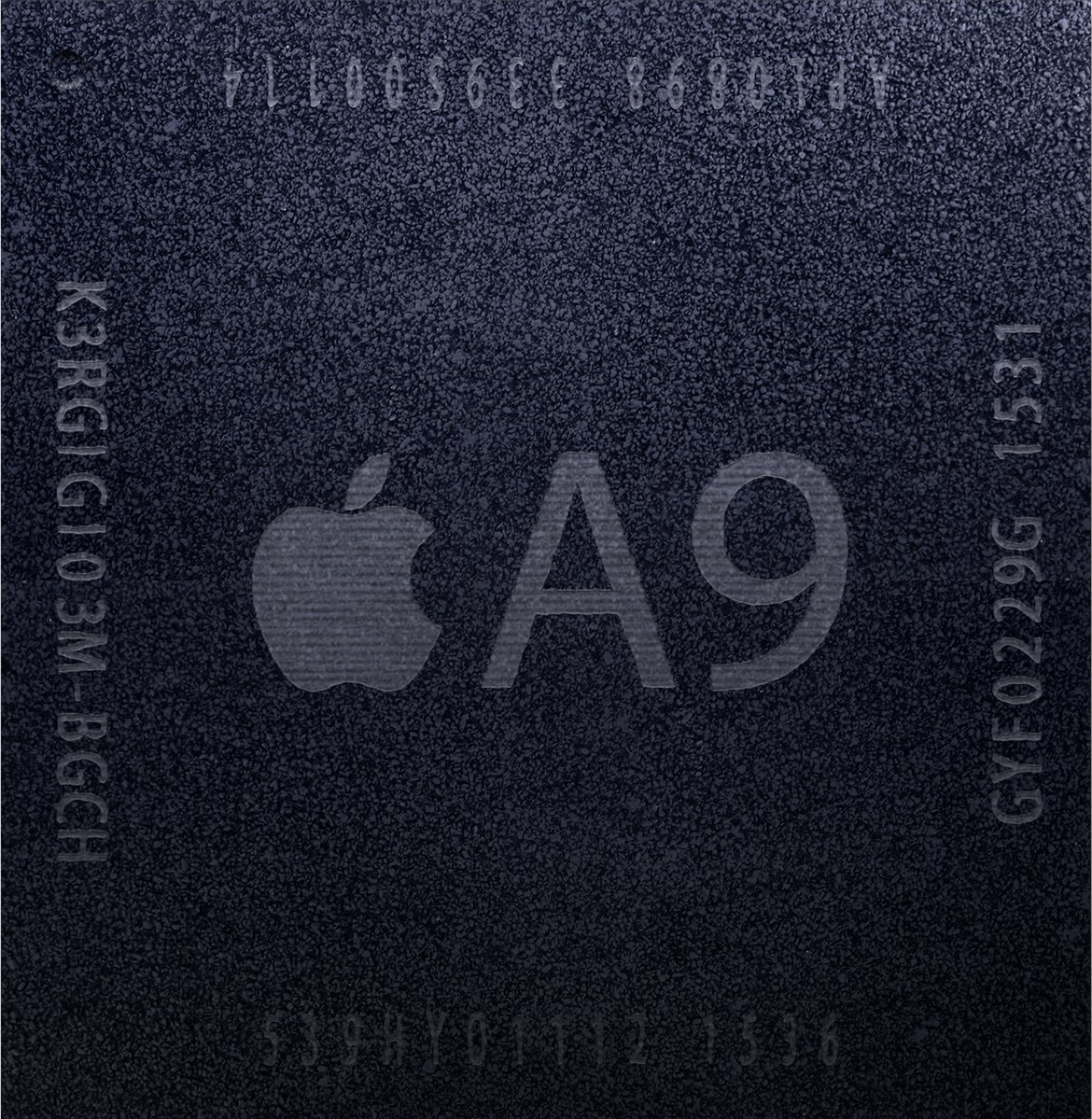
A9
".... Apple A9 chips are
fabricated by two companies:
Samsung and
TSMC. The Samsung version is called APL0898, which is manufactured on a 14 nm
FinFET process and is 96 mm2 large, while the TSMC version is called APL1022, which is manufactured on a 16 nm FinFET process and is 104.5 mm2 large. ..."

en.wikipedia.org
A10
"... he A10 (internally, T8010) is built on TSMC's 16 nm
FinFET process
[1][9] and contains 3.28 billion transistors (including the GPU and caches) on a die size of 125 mm2.
[10] .."
en.wikipedia.org
The A10 'bloated' up to "iPad Pro" A--X / M1 size and hasn't been that big since. [ The A10X had to jump to TSMC 10nm to stay in the 120-140mm^2 zone for a 'bigger A series' offering. ]
The A10 probably got some die space layout uplift because it was not dual sourced. but did Apple "effiecenly" save space to add substantive new features is on thin ice for evidence ( it is a bigger die). Did they make a bigger die that usually showed no increase in power levels. Yes. Did they save die space? No. ( got better at turning stuff not being used off. )
The problem with A16/M2 staying with TSMC N5 generation is that they have already done that. A14 (TSMC N5) and A15 ( pretty good chance was already on N5P. ). Apple took a die 'bloat' here also. A14 ( 88mm^2 ) and A15 ( 107mm^2 )
Despite TSMC’s claims of a 1.35x shrink on SRAM, Apple’s system cache has only shrunk 1.22x. This has far reaching implications for the industry. Designers cannot use increased LLC sizes as a crutc…

semianalysis.com
TechInsights released a die shot of the A15 and with the help of SkyJuice’s, we are analyzing it today.

semianalysis.substack.com
The notion that would keep N5 density and go to a > 107mm^2 for A16 and likewise grow the M2 past the normal "iPad Pro" die size is dubious when there is a N4 process with a 6% shrink readily available. ( MediaTek and Qualcomm are using it this year. Why would Apple skip it for A16 when had already bloated up on A15? That would mean more wafers to make the same amount of die. )
Apple hasn't stuck around for
three iterations on the same process general node before. The notion that "well they have done two generation in the past"... yeah. But this wouldn't be two. They have already done two. The real illustrative past example would be looking for is 3. ( N5P gets no density improvements to "add more stuff". It is a power utlization update where can either incremental bump the clock speeds (and use same power) or use less power ( and keep same clock. ). Apple did a little of both of those with A15 )
The best example is probably nVidia's Maxwell 2 generation GPUs which nearly doubled the performance of the previous Kepler generation GPUs without significantly increasing power consumption while using the same TSMC 28 nm process through a comprehensive architectural redesign.
GM206 (maxwell 2.0 512 shaders ) 228mm^2
GM107 (Maxwell 640 shaders ) 148mm^2
Maxwell 2.0 also largely went much, much bigger to get more power. Yes the new tweaks allowed the thermals not to spin out of control, but if use lots more die then should expect more performance if doing anything remotely competent. (more cache, execution units transistor budget allocation, more fixed function logic , etc. )
Marketing can always work around previous statements if they wanted to. For example, if they wanted to save the "M2" term for a true architectural successor to the M1 line, they could just add a suffix to brand new refreshed/minor-enhanced M1 chips like M1E for enhanced. It could even be a whole line if required like M1E Pro and M1E Max. Calling it something like the M1E line would still be consistent with their statement that the M1 line is done.
Why would marketing want to "save the M2" tag if the M1 is almost two year stale? Apple is about to hit they front edge of their "two year transition" timeline window sitting on the exact same "M1" they started off with. That is clearly
not showing progress.
It isn't Apple who has a big bug up their but on the "M2 has to be some giant leap" notion. It is the tons of folks on these forums who have pushed the notion that Apple is insanely better designers than everyone else and M-series is going to take over the PC world . Apple is good, but they have always been riding on a 18 month Moore's law cycle to make major contributions to their year-over-year run up on performance. When that slide out closer to 24 (or 30 months) the pace will slow down. Apple isn't going to engineer those contributions back in and still keep the die costs in the same ballpark. (And yes Apple probably does have a die size and cost constraints on these dies. Pro/Max get bigger budgets but also likely have a 'cap' also on costs. )