filmbuff
macrumors 6502a
I heard Big Sur will be followed by future versions of Mac OS too.
Seems like GAAFET (Gate All-Around FETs) are the answer at below 5 nm. Pretty interesting transistor design - utilizing carbon nanowires with the gate wrapping around them.Yes, they can go sub-nanometer. They can keep going until quantum effects prevent the ability to shut of the transistor gate. As they get smaller they will modify the gate geometries (which they’ve already done once, when they moved to FINFETs instead of MOSFETs) in order to provide a stronger electrical field to shut off the gate. At some point they may have to go to vertical transistors, like bipolar devices, where the layer thicknesses are the critical dimensions (since those are easier to control). At the point where they can finally go no further, they may have to switch to semiconductors with heterojunctions (e.g. GaAs or InP) in order to increase carrier mobility without shrinking the gates further. Or they can use bandgap engineering with silicon (which already occurs - most process now use germanium to modify the bandgap).
It will be quite awhile before things hit a dead end.
Very important, yes. Exciting, also yes. But revolutionary? Perhaps down the line, but so far EUV has just allowed these fabs to make pretty minor, incremental, evolutionary improvements. I guess they all add up over 5-10 years, though! TSMC must own over half the EUV ASML machines in existence at this point.This is revolutionary. The reason 5 nm took so long is because traditional 193 nm ArFi DUV lithography (the process by which light is used to pattern wafers using photoresist) needed multiple patterning to achieve 10 nm. Now that EUV, which has been in development by ASML for over 25 years is finally ready, we can finally scale down to sub 7 nm, without the need for multiple patterning. Even more exciting is when ASML will release their high-NA EUV tools next year, we'll be seeing bigger jumps and node shrinks.
ASML is one of the most important companies on planet earth now, and few even know it exists.
Could be. Or MBCFET. Or any of a large number of other choices that all operate on the same principle of applying the electrical field to gate from more directions. Not sure 4nm is where they have to do it, but they’ll need to do it before 2030 probably.Seems like GAAFET (Gate All-Around FETs) are the answer at below 5 nm. Pretty interesting transistor design - utilizing carbon nanowires with the gate wrapping around them.
Revolutionary, yes. Shrinking the light source from 193 nm to 13.5 nm is a gargantuan step. To produce at 10 nm, upto quadruple patterning (with multiple litho-etch steps) was used. EUV simplifies this process tremendously, and on N5, a lot more layers of EUV are being used. It's the biggest improvement in lithography we've seen yet, 5 nm simply would not be possible without it.Very important, yes. Exciting, also yes. But revolutionary? Perhaps down the line, but so far EUV has just allowed these fabs to make pretty minor, incremental, evolutionary improvements. I guess they all add up over 5-10 years, though! TSMC must own over half the EUV ASML machines in existence at this point.
Very exciting! The jump from N5 to N3 will be massively significant. I believe it will primarily depend on ASML's new high-NA EXE 5000 system, which will allow for smaller patterns to be resolved. TSMC has been very aggressive with EUV implementation, and it shows. Intel and Globalfoundries have all but given up on EUV, and seem to have let DUV play its course. Fabs simply cannot ramp up fast enough to accommodate 5 nm for all vendors - it takes a couple years to tool for EUV, and ASML's order book is backed up quite a bit.AnandTech Forums: Technology, Hardware, Software, and Deals
Seeking answers? Join the AnandTech community: where nearly half-a-million members share solutions and discuss the latest tech.www.anandtech.com
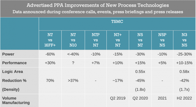
Here is the timeline released my TSMC themselves.
And the performance and battery life increases are stunning. I think I'll wait for the M3. When Apple says the transition will be over in 2 years, this is what they mean:
That would be physically impossible as the size of an atom of silicon is .2nm. But we can surely see some wafers which are less than 3nm. You would have to move on to another element, or go quantum.Waiting for 0nm processor
Yes, they can go sub-nanometer. They can keep going until quantum effects prevent the ability to shut of the transistor gate. As they get smaller they will modify the gate geometries (which they’ve already done once, when they moved to FINFETs instead of MOSFETs) in order to provide a stronger electrical field to shut off the gate. At some point they may have to go to vertical transistors, like bipolar devices, where the layer thicknesses are the critical dimensions (since those are easier to control). At the point where they can finally go no further, they may have to switch to semiconductors with heterojunctions (e.g. GaAs or InP) in order to increase carrier mobility without shrinking the gates further. Or they can use bandgap engineering with silicon (which already occurs - most process now use germanium to modify the bandgap).
It will be quite awhile before things hit a dead end.
That would be physically impossible as the size of an atom of silicon is .2nm. But we can surely see some wafers which are less than 3nm. You would have to move on to another element, or go quantum.
Came her me to ask this exact question lolI’m curious, how far can they go with shrinking nodes? Is sub-nanometer a thing? If it isn’t, how does the industry move on from silicon
Remember too that 5nm doesn’t mean any gates are actually 5nm wide. The node names have different meanings at different fabs, but usually they are somewhat correlated with the smallest possible feature size, and transistor gates are bigger than that.
It’s probably no accident that Intel ran into issues going to 10nm. TSMC might hit a wall at 4nm for all we know. At some point the laws of physics override Moore’s Law.

BothOh, boy. What iPhone to buy? 13 or 14? 🤔
TSMC has timetable for 3nm process and are planning for 2nm plant in northern Taiwan. However I do wonder when they will stop counting by nm. Maybe we will use number of atoms instead for the future.
TSMC to build 2nm wafer plant in Hsinchu - Focus Taiwan
Taipei, Sept. 23 (CNA) Taiwan Semiconductor Manufacturing Co. (TSMC), the world's largest contract chipmaker, said Wednesday it will build a sophisticated 2 nanometer wafer plant in Hsinchu.focustaiwan.tw
I wonder what the theoretical limit is before transistors stop working due to quantum fluctuations
According to this article, Samsung will gate-all-around in 2022 for their 3nm process & TSMC will adopt the same in 2024Could be. Or MBCFET. Or any of a large number of other choices that all operate on the same principle of applying the electrical field to gate from more directions. Not sure 4nm is where they have to do it, but they’ll need to do it before 2030 probably.

GAA is what Samsung & TSMC will relying on starting in 2022 & 2024 respectively.Seems like GAAFET (Gate All-Around FETs) are the answer at below 5 nm. Pretty interesting transistor design - utilizing carbon nanowires with the gate wrapping around them.
I don't have a good picture of what transistors look like, so I found this simplified cartoon, pasted below, at https://semiengineering.com/transistor-options-beyond-3nm/It’s not a matter of the name of the process. And “5nm” is just a name, it’s not the size of the transistor gate. They can get quite a bit smaller before they get stuck. Changing the gate structure so that the electric field can be applied from all sides will help.
We already worry about quantum effects - we have been dealing with them for at least 10 years. It’s part of why we have static leakage current even when devices are shut off.