I just got rid of my 2019 16" and replaced it with an M1 13". It's running at 33.8C right now. When I'm really hammering it I've seen 40.5C max. Just incredible.
Got a tip for us?
Let us know
Become a MacRumors Supporter for $50/year with no ads, ability to filter front page stories, and private forums.
Apple Supplier TSMC Readies 3nm Chip Production for Second Half of 2022
- Thread starter MacRumors
- Start date
- Sort by reaction score
You are using an out of date browser. It may not display this or other websites correctly.
You should upgrade or use an alternative browser.
You should upgrade or use an alternative browser.

IBM doesn't manufacture semiconductors any more. That article is about a research prototype, not something shipping in volume.IBM is actually ahead of them, they are on 2nm.
IBM Unveils World's First 2 Nanometer Chip Technology, Opening a New Frontier for Semiconductors
IBM (NYSE: IBM) today unveiled a breakthrough in semiconductor design and process with the development of the world's first chip announced with 2 nanometer (nm) nanosheet technology....newsroom.ibm.com
Does it mater when the performance is still there either way, as it unarguably is? In fact, if it means they won't be bottlenecked by the laws of physics for longer this could actually been as a good thing...If only the 3nm process actually had 3nm transistors. It's only marketing unfortunately, no feature on the wafer is actually 3nm.
No. All new chips improve efficiency by a combination of architectural gains and process gains. Just because M1 is fast and efficient, doesn't allow any specific statement about process characteristics.The M1 proves that you are wrong
These improvements of perf/efficiency in a process have long been exclusive - look it up. It says so in the linked article btw but was quoted wrongly ("alongside" which at least I'd interpret as "and" in that case.)
Original article:
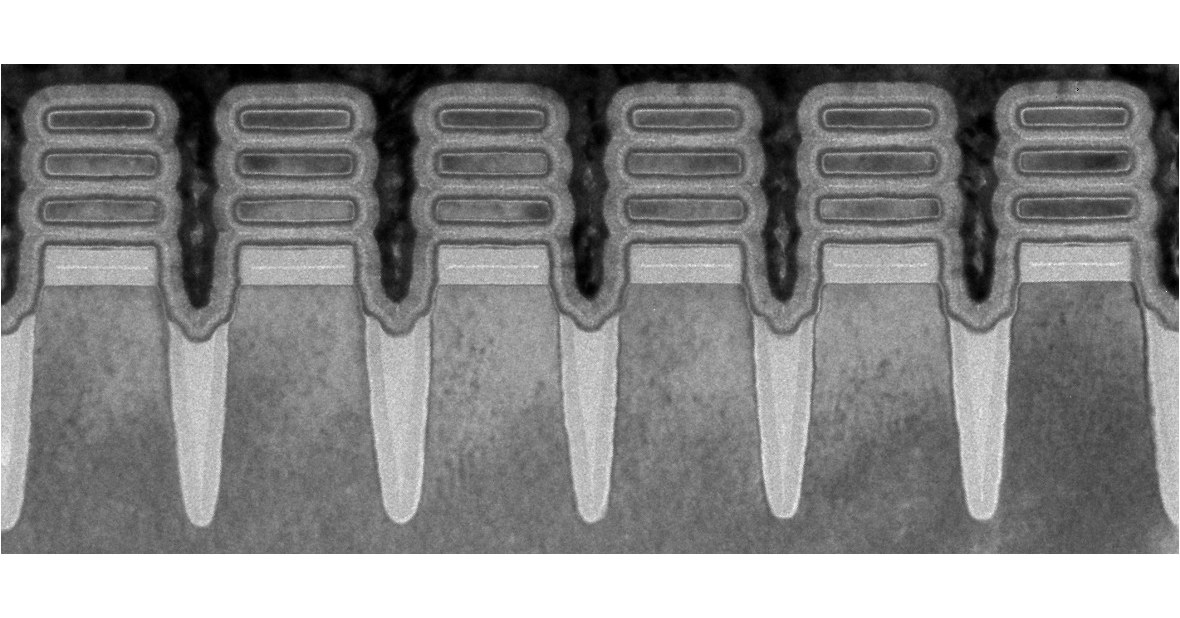
TSMC has claimed its N3 technology will be the world's most advanced technology when it begins volume production in the second half of 2022. Relying on the proven FinFET transistor architecture for the best performance, power efficiency, and cost effectiveness, N3 will offer up to 15% speed gain or consume up to 30% less power than N5, and provide up to 70% logic density gain.
No. All new chips improve efficiency by a combination of architectural gains and process gains.
You, earlier:
Article is not correct - it's either 15% speed gain OR 30% less power. Never both - people always seem to confuse this.
M1 is a smaller process and a newer microarchitecture.
True, so? Doesn’t contradict my earlier post.You, earlier:
M1 is a smaller process and a newer microarchitecture.
Actually what matters more than anything is ACHIEVED density.Intel 7nm is more dense than TSMC 5nm.
Routed gate density matters more than anything.
Intel's density claims are uninteresting because they do not match (not even close, they're off by a factor of 2 to 3) any product that Intel actually ships...
So why does Intel boast about them? WTF knows -- I guess to impress the rubes.
Who is "they"?I wish they would just stop with the marketing hype.
3nm does not mean every or even most features are that size. It literally means nothing these days.
What is the gate density?
A 5nm design with 10 metal layers will have higher density than 3nm with half the metal layers.
Intel, yes, lots of hype -- but nothing around 3nm.
Samsung, too much hype -- they are on the Intel track where they start to care more about the hype than the reality.
IBM some hype.
Show me an instance of TSMC *hype*. It's all sober analysis, graphs, numbers.
That's a silly analysis.As usual, IBM is about the theoretical just like their useless big blue machine.
There is a lot of interesting technology in z/series. They are designed to perform a very different type of task from Apple or Intel CPUs, leading to different (but not stupid) choices. Items of particular interest include
- the cache coherence protocol (taking account of the multiple levels of cache and the hierarchy of CPUs across chips then boards then racks)
- the virtual L1 cache and its tight integration with the L2
- the 2nd level branch prediction and how that is closely tied to instruction prefetch
The first of these is unlikely to be of much interest to Apple; the second and third include ideas that I could well see Apple using in the future.
I think I read an article here saying a jet fighter has a G5 CPU.
I read in Jane's (a major defense industry publication) back in the early 2000s that USAF F-15s and F-16s had been upgraded to use PPC 7400 (G4) CPUs. It would be reasonable to assume that they had been updated to G5 CPUs later on.
Yes it does. The M1 is a speed gain and draws less power.True, so? Doesn’t contradict my earlier post.
Article is not correct - it's either 15% speed gain OR 30% less power. Never both - people always seem to confuse this.
Not exactly.
What you are saying is true for an individual transistor, or a collection of identical transistors, but it isn't necessarily true for a design.
A good design will use a range of transistors from the fastest that are appropriate sitting in critical paths, to the lowest power that can still do the job, sitting in non-critical paths. The next version of the design can run its "fast" transistors 15% faster, its "low power transistors" at 30% lower power, and achieve gains on both axes. To the extent that the critical path transistors control most of performance, you can be 15% faster, while, to the extent that much (not, most, that would be overstating it) power is dissipated in the low power transistors, that power is down by 30%. You might be able to get something like device is 12% faster at 18% lower power.
.....
Even that understates the case because it assumes a pure port of an existing design. Smarter would be a revised design that plays to the strength of the new process; most likely insofar as it makes even more use of stored state (larger caches, branch predictors, etc). Even better (but much more difficult for an outsider to judge) is situations where the new process allows for "crossing a cliff" -- the way the power vs frequency played out with the old process, the maximum width of your renamer at the frequency you want was 8 wide, but the new process allows you to bump this to 10-wide without that either becoming an unbearable hot-spot, or forcing the clock too slow.
My guess (only a guess) goes as follows
- Apple seems to have a "complete" design cycle time of about 4 years. Meaning that the pattern to expect is something like
- first design, 3 iterations, next design, 3 iterations, ...
- we've been through two rounds of this (A7/8/9/10 6-wide, with constant refinement; then A11/12/13/14 now 8-wide, designed from the start as asymmetric with two core complexes, little core a reparameterization of the big core)
- in both cases the first member of the set was designed with all the most difficult parts scaled correctly, and then extra pieces filled in via refinement. So A7 was 6-wide, but subsequent versions added more FP pipelines, a second int multiplier and so on
- so my guess is that (assuming the cycle wasn't delayed a year because of all the addition complexities around the x86/mac transition) A15 will be a different design *at the lowest levels*. It may not superficially look different because only the bones have changed; it will be the A16 and later than add onto those bones. So, eg, width may be increased to 10-wide, but not the number of execution units. 4xNEON may be reconfigured to 2xSVE256, but we don't actually get more basic FMAC capability. Virtual registers are added -- but no additional physical registers yet. etc etc
- point is this is what I mean by redesign. The design looks like mostly unchanged. Same frequency, maybe 20% better IPC, main change looks like SVE and ARMv9 capabilities (MTE, BTI etc). BUT new design has exploited BOTH the 15% speed boost and the 30% lower power to rework all the most critical areas (rename, schedule) to operate more aggressively, and we then see that play out in further 15% IPC boost over the next three cores, which will occasionally take a process boost primarily in frequency.
IBM certainly is still in the game, but in the part of the game they find most profitable. Multiple IBM Power 9 systems are on the list of the Top-500 Supercomputers in the world. And IBM Z series mainframes are still used by the biggest banks and airlines. When you can still sell multi-multi-million dollar systems, why settle for building CPUs that run in consumer laptops, earbuds, and smart watches. That's Apple's part of the game.Though I thought IBM is out of the CPU game for reasons I do not understand
There potentially might be a tiny crossover when Apple eventually ships a new top-of-the line Apple Silicon Mac Pro, which might benchmark in the same magnitude range an IBM's bottom entry-level Power 9 systems.
IBM certainly is still in the game, but in the part of the game they find most profitable. Multiple IBM Power 9 systems are on the list of the Top-500 Supercomputers in the world.
They don't manufacture those any more (GlobalFoundries bought their fabs), which is what was being discussed here.
It is astonishing how fast technology evolves.
And yes, I find miniaturization of electronics innovative.
Yep... This should give Intel a run for 'someone's' money..
Despite them struggling with 7nm, Intel would still go to 5, 3 and 1.4nm, i read, by 2029 as a roadmap

Despite 7nm Struggle, Intel to Keep Investing in 5nm, 3nm Chip Technologies
Intel CEO Bob Swan says the company will remain an integrated devices manufacturer, even as it mulls whether to outsource its 7nm chip production to a third-party foundry.
While all that sounds good, (on paper) ...Apple would just turn off that light asap
This article makes it sound like it's all about TMSC's tech. It's more accurate to say this resulted from a successful collaboration between TMSC and ASML; ASML produces the EUV lithography machines that enable the 3 nm tech. Of course, Intel also has access to these machines, but they've not succeeded where TMSC has.
 www.tomshardware.com
Intel, Samsung, and TMSC have all been heavily involved with ASML:
"In 2012, Intel, Samsung and TSMC all invested heavily in ASML as a way to jump-start development of extreme ultraviolet (EUV) lithography, with Intel sinking in $4 billion to acquire a 10% stake."

 www.eetimes.com
ASML and TSMC Reveal More Details About 3nm Process Technology
TSMC's N3 node to use EUV extensively
Intel, Samsung, and TMSC have all been heavily involved with ASML:
"In 2012, Intel, Samsung and TSMC all invested heavily in ASML as a way to jump-start development of extreme ultraviolet (EUV) lithography, with Intel sinking in $4 billion to acquire a 10% stake."
Intel Again Cuts Stake in ASML - EE Times
U.S. chip giant cuts investment in Dutch lithography vendor to below 3% of the company's outstanding shares, according to a regulatory filing.
They are ahead of the completion. By 2 nodes.Lol, it’s not even 3nm. They are lying to appear ahead of the competition.
They don't manufacture those any more (GlobalFoundries bought their fabs), which is what was being discussed here.
So what does IBM do any more?
I read in Jane's (a major defense industry publication) back in the early 2000s that USAF F-15s and F-16s had been upgraded to use PPC 7400 (G4) CPUs. It would be reasonable to assume that they had been updated to G5 CPUs later on.
more interestingly, who would still be manufacturing G5 CPUs now?
So what does IBM do any more?
more interestingly, who would still be manufacturing G5 CPUs now?
IBM still designs CPUs, researches semiconductor technologies, designs and sells workstations and mainframes, artificial intelligence, etc.
I never said anything was important.Since when did pitch become the important metric?
I simply stated this is problem with using abritrary numbers for node sizes, so who don't do any research will just compared 10 > 7 must be worse because one number is bigger than the other. It's like comparing car engines and just looking at displacement without any consideration to anything else.
You said they aren’t behind at all, because of the pitch. So let me rephrase my question - what makes you think that “pitch” determines whether they are behind or not?I never said anything was important.
I simply stated this is problem with using abritrary numbers for node sizes, so who don't do any research will just compared 10 > 7 must be worse because one number is bigger than the other. It's like comparing car engines and just looking at displacement without any consideration to anything else.
I think you may be confusing "ready for production" with a design concept lolIBM is actually ahead of them, they are on 2nm.
IBM Unveils World's First 2 Nanometer Chip Technology, Opening a New Frontier for Semiconductors
IBM (NYSE: IBM) today unveiled a breakthrough in semiconductor design and process with the development of the world's first chip announced with 2 nanometer (nm) nanosheet technology....
Register on MacRumors! This sidebar will go away, and you'll see fewer ads.