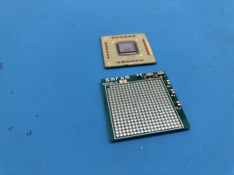
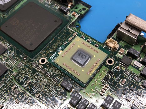
Another weird update/oddity... The NVRAMRC script, unmodified, actually works FINE, but NOT when it is executed automatically on boot (with use-nvramrc? set to true). If you set the NVRAMRC script (but use-nvramrc? to false), then execute the NVRAMRC manually in OF (run "nvramrc evaluate"), it actually works just fine. Very, very odd.
Got a tip for us?
Let us know
Become a MacRumors Supporter for $50/year with no ads, ability to filter front page stories, and private forums.
"fastest" flash, and using a pencil to overclock.
- Thread starter Reflex88
- Start date
- Sort by reaction score
You are using an out of date browser. It may not display this or other websites correctly.
You should upgrade or use an alternative browser.
You should upgrade or use an alternative browser.
You can use "multi-boot" instead, which will show the boot picker instead of just booting right away.Ah, ok. I was trying an external firewire drive. I guess I need to figure out how to do that in OF or else physically change the drive so that "mac-boot" picks the correct one...
I can confirm this on a Mini 10,2 with a 7448. I'm very grateful for your efforts dosdude1!

In terms of real world speed difference, does it matter much 7448 and 7447 ? If so, then I may be interested in the 7448 on my DLSD 15 inch.
Another huge update: I FULLY FIXED the NVRAMRC script, and it can now be loaded on boot automatically without issue! I have attached a text file containing the updated script; just set it as NVRAMRC using Terminal in Mac OS. Then you should be able to set use-nvramrc? to true as well, and the system should still boot successfully, along with properly detecting an installed 7448! Video demo here:
Although it ended up being unnecessary, I did also spend the time to FULLY reverse-engineer and re-implement the FCode binary source, which I have also attached. It ended up not being the issue, so no modifications actually needed to be made to it.
Although it ended up being unnecessary, I did also spend the time to FULLY reverse-engineer and re-implement the FCode binary source, which I have also attached. It ended up not being the issue, so no modifications actually needed to be made to it.
Attachments
Last edited:
very awesome to see you managed to fix the issue in the end! and reverse-engineer the fcode part of thingsAnother huge update: I FULLY FIXED the NVRAMRC script, and it can now be loaded on boot automatically without issue! I have attached a text file containing the updated script; just set it as NVRAMRC using Terminal in Mac OS. Then you should be able to set use-nvramrc? to true as well, and the system should still boot successfully, along with properly detecting an installed 7448! Video demo here:
Although it ended up being unnecessary, I did also spend the time to FULLY reverse-engineer and re-implement the FCode binary source, which I have also attached. It ended up not being the issue, so no modifications actually needed to be made to it.
I can see some fun upgrades happening in the future on a number of machines
@ervus Did you get a chance to try this modified script? If so, let me know if it works as intended on your machine.Another huge update: I FULLY FIXED the NVRAMRC script, and it can now be loaded on boot automatically without issue! I have attached a text file containing the updated script; just set it as NVRAMRC using Terminal in Mac OS. Then you should be able to set use-nvramrc? to true as well, and the system should still boot successfully, along with properly detecting an installed 7448! Video demo here:
Although it ended up being unnecessary, I did also spend the time to FULLY reverse-engineer and re-implement the FCode binary source, which I have also attached. It ended up not being the issue, so no modifications actually needed to be made to it.
Yes, it works on the Mini 10,2 the same as the FCode.bin from a USB stick. Thanks again!
Has anyone tried it on a DLSD?
Has anyone tried it on a DLSD?
I have, and it works as intended on there as well.Yes, it works on the Mini 10,2 the same as the FCode.bin from a USB stick. Thanks again!
Has anyone tried it on a DLSD?
Out of curiosity, does any of the incredible work done here mean anything for the prospect of better/more readily available CPU upgrade cards for PowerMac G4s?
I know there were commercial 7448-based upgrades for the earlier G4s with the 133 MHz bus, but they've always seemed hard-to-find and painfully expensive. Would be very cool if we now had the collective knowledge to retrofit the OEM CPU cards with fast and relatively cheap modern G4s!
I know there were commercial 7448-based upgrades for the earlier G4s with the 133 MHz bus, but they've always seemed hard-to-find and painfully expensive. Would be very cool if we now had the collective knowledge to retrofit the OEM CPU cards with fast and relatively cheap modern G4s!
The upgrade "cards" are pretty much figured out already by the aftermarket companies like sonnet, etc. We are trying to upgrade other G4 computers like the Mini, PowerBook, etc. by soldering in faster chips. This is where the firmware hacks come into play, because the aftermarket patching utilities don't always work on these machines.
For "cards" there are the usual places like eghey and various forum classifieds:
forums.macrumors.com/threads/where-to-find-g4-cpu-upgrades-in-2021.2326264/
forums.macrumors.com/threads/is-it-possible-to-upgrade-the-dual-cpus-in-a-450-mhz-graphite-gigabit-ethernet-power-mac-g4.2333438/
For "cards" there are the usual places like eghey and various forum classifieds:
forums.macrumors.com/threads/where-to-find-g4-cpu-upgrades-in-2021.2326264/
forums.macrumors.com/threads/is-it-possible-to-upgrade-the-dual-cpus-in-a-450-mhz-graphite-gigabit-ethernet-power-mac-g4.2333438/
I plan to make my own CPU upgrade card at some point, based on the design of the Sonnet dual-1.8 GHz card. It will support a dual-7448 configuration, and work in all the older PowerMac G4s, including the G4 Cube.Out of curiosity, does any of the incredible work done here mean anything for the prospect of better/more readily available CPU upgrade cards for PowerMac G4s?
I know there were commercial 7448-based upgrades for the earlier G4s with the 133 MHz bus, but they've always seemed hard-to-find and painfully expensive. Would be very cool if we now had the collective knowledge to retrofit the OEM CPU cards with fast and relatively cheap modern G4s!
I'm willing to send my eMac motherboard to someone who can swap it with a 7448, but I'm not sure exactly what to do first. I know the bootrom is 4.9.2 or something and I did set the vcore to 1.375V and set the PLLs for the CPU to run at 1.92GHz. All that may need to be changed as the 7447B takes more power than a 7448. Maybe I could get it to 2.08GHz? But I am not sure.
Forgot to post here when I initially did this, but recently I got a 7448 CPU working in a Titanium PowerBook G4, by way of using a custom interposer PCB designed by “Herd” on 68kmla. This PCB converts the footprint and pinout of a 745x CPU to that of a 744x, allowing the installation of any 744x CPU! This particular TiBook, having a 7451 originally but without any provisions for the backside L3 cache, was the perfect candidate for such a swap (as normally you lose L3 cache support going from 745x to 744x). In the end, I was able to get the machine running stably with a 7448 at 1.73 GHz, a MASSIVE upgrade from this machine’s original 667 MHz 7451!


Nice proof of concept, but at the same time I'm wondering how long will it take until the adapter PCB deform and lose some of the contacts due to thermal expansion.
Anyone ever wondered why manufacturers are using ceramic substrates and epoxy fill around the edges of the chips? And use tightly controlled tepmerature profiles during manufacture?
I bet, that TiBook will be dead sooner rather than later..
Anyone ever wondered why manufacturers are using ceramic substrates and epoxy fill around the edges of the chips? And use tightly controlled tepmerature profiles during manufacture?
I bet, that TiBook will be dead sooner rather than later..
Last edited:
PCBs don't start deforming or warping to that degree until they get up to around 280 - 300 degrees C (and even then they generally don't warp all that much), which of course it will never even come close to under normal operation. So no, the PCB warping and breaking solder joints is highly unlikely to ever happen in this system.Nice proof of concept, but at the same time I'm wondering how long will it take until the adapter PCB deform and lose some of the contacts due to thermal expansion.
Anyone ever wondered why manufacturers are using ceramic substrates and epoxy fill around the edges of the chips? And use tightly controlled tepmerature profiles during manufacture?
I bet, that TiBook will be dead sooner rather than later..
Awesome work!
^ any news on this by any chance?I plan to make my own CPU upgrade card at some point, based on the design of the Sonnet dual-1.8 GHz card. It will support a dual-7448 configuration, and work in all the older PowerMac G4s, including the G4 Cube.
I love the idea of making new hardware for vintage machines and this is especially intriguing to me. Have you given much more thought to this or considered any community collaboration and/or open sourcing of the design? I'd love to help out with this if there is anything that I might be able to contribue my experience or resources towards. I have a fair amount of experience designing compact power supplies (and I really enjoy doing it). I also have everything needed to do small-batch surface mount PCB production. I don't have a ton of confidence that I could build a CPU card entirely on my own though. I don't really have any experience designing for high-speed, high-density interconnects like are involved in a CPU card; but I know that there are dragons there.I plan to make my own CPU upgrade card at some point, based on the design of the Sonnet dual-1.8 GHz card. It will support a dual-7448 configuration, and work in all the older PowerMac G4s, including the G4 Cube.
I got a 7448 CPU working in a Titanium PowerBook G4
Wow, that's amazing work! Thanks for sharing your result!
The issue I'm facing right now is figuring out the pinout of the 300-pin MPx bus connector on the CPU boards. Should be relatively trivial to figure out though; just need to sit down for a few hours and do some continuity tests on a stock CPU board. From there, the actual schematic and new design can be made.I love the idea of making new hardware for vintage machines and this is especially intriguing to me. Have you given much more thought to this or considered any community collaboration and/or open sourcing of the design? I'd love to help out with this if there is anything that I might be able to contribue my experience or resources towards. I have a fair amount of experience designing compact power supplies (and I really enjoy doing it). I also have everything needed to do small-batch surface mount PCB production. I don't have a ton of confidence that I could build a CPU card entirely on my own though. I don't really have any experience designing for high-speed, high-density interconnects like are involved in a CPU card; but I know that there are dragons there.
I can certainly do the swap for you, though I do not have an eMac chassis to actually test it. So it will be up to you to test different PLL configs and appropriately modify CPU VCORE voltage. You will first of course need to patch the system's BootROM before doing anything. You can try using the GigaDesigns patch, but if that doesn't work, the ROM will most likely need to be manually patched. I can do so for you; you just need to dump the machine's BootROM using my custom Flashrom build under Linux (I normally use Ubuntu Mate 16.04), and send it to me. Then you can flash my modified version back on again using Flashrom.I'm willing to send my eMac motherboard to someone who can swap it with a 7448, but I'm not sure exactly what to do first. I know the bootrom is 4.9.2 or something and I did set the vcore to 1.375V and set the PLLs for the CPU to run at 1.92GHz. All that may need to be changed as the 7447B takes more power than a 7448. Maybe I could get it to 2.08GHz? But I am not sure.
Looks like they are Amphenol MEG-Array connectors? I only have a dual 7400 that I'm willing to disassemble right now. I know the early G4 360 BGA chips had a different pinout, but as far as I'm aware, the pins on the mezzanine connector are identical across all of the G4 cards. So what we really need to know is just which BGA pads connect to which pins on the mezz? I suppose the traces from the mezz to the BGA might be different depending on the processor model though... I could add a socket to my next component order and design a break-out board for it to make it easier to probe out the connections. Maybe I'll probe it out if I have a slow weekend soon. If it works out okay and helps save time on the process, I'd be happy to ship it out to someone who is willing to remove the chips on a 744-based card and probe it.The issue I'm facing right now is figuring out the pinout of the 300-pin MPx bus connector on the CPU boards. Should be relatively trivial to figure out though; just need to sit down for a few hours and do some continuity tests on a stock CPU board. From there, the actual schematic and new design can be made.
Last edited:
I've actually already found the necessary connector, and found a source to buy them when the time comes. It should be as simple as removing the CPU, looking at a datasheet for said CPU, and continuity testing every single pin of the MPx bus connector to the CPU pads. Though I found in my initial testing doing this that the address lines (and maybe other lines) have some sort of resistance between the MPx connector pin and respective CPU pad, probably series termination resistors or something. Haven't spent enough time to sit down and map it all out though, but if you are willing to work on the schematic/board design with me, I'll do that sooner rather than later to get an initial schematic started (should have time this weekend). I've already got a couple CPU boards with CPUs removed to do just this. From that point, no (or very minor) further reverse engineering will be required. I do plan to make this whole design open-source.Looks like they are Amphenol MEG-Array connectors? I only have a dual 7400 that I'm willing to disassemble right now. I know the early G4 360 BGA chips had a different pinout, but as far as I'm aware, the pins on the mezzanine connector are identical across all of the G4 cards. So what we really need to know is just which BGA pads connect to which pins on the mezz? I could add a socket to my next component order and design a break-out board for it to make it easier to probe out the connections. Maybe I'll probe it out if I have a slow weekend soon.
How many do you want to make? I saw some of the sonnet boards are for sale. You could just solder parts to them, or if you want to copy the design you could sand one down and take pictures of the layers.
www.ebay.com/itm/153437679896

www.ebay.com/itm/153437679896
I have a huge update regarding this: After painstakingly buzzing out every single pin, I have successfully mapped out pretty much the entirety of the 300-pin MPx Bus connector! I then created the correct schematic symbol and footprint, and have started working on the initial schematic, which is available on my GitHub here: https://github.com/dosdude1/MPx-CPU-Board-744x (it is a KiCad 6.x project).Looks like they are Amphenol MEG-Array connectors? I only have a dual 7400 that I'm willing to disassemble right now. I know the early G4 360 BGA chips had a different pinout, but as far as I'm aware, the pins on the mezzanine connector are identical across all of the G4 cards. So what we really need to know is just which BGA pads connect to which pins on the mezz? I suppose the traces from the mezz to the BGA might be different depending on the processor model though... I could add a socket to my next component order and design a break-out board for it to make it easier to probe out the connections. Maybe I'll probe it out if I have a slow weekend soon. If it works out okay and helps save time on the process, I'd be happy to ship it out to someone who is willing to remove the chips on a 744-based card and probe it.
I'm hoping to have the end result be a dual-744x board, but I may abandon the idea of having two CPUs if it ends up being significantly more difficult to design and/or route, or much more expensive to produce.
At this point, I have now put in over 20+ hours working on this (mapping out the connector took me the best part of 3 days), and it is at the point now where I am ready to start working on the supporting circuitry design, such as VCORE regulator, decoupling, implementing all the necessary pullups/pulldowns, etc.
Now, with that said, it definitely would be beneficial if you or someone could double-check the pinout, by buzzing everything out again on another card (NOT an MDD card, as they have a different pinout... As I found out the hard way). I'm 90% sure it's all correct (I went over it a second time after the initial mapping), but it's always best to have a second pair of eyes go over something like this. It's about 130 lines to probe, so it's very time-consuming.
With regard to the CPU VCORE supply design, if you would be willing to work on that, that would be absolutely awesome. It's the one part of this I have the least experience with, so having you assist with that would be very helpful. The only note I have to add is that I'd prefer using a buck regulator that has its output voltage set via "VID" pins on the regulator, rather than by changing resistor values as some designs employ (such as the one used in the iMac G4). It makes it much easier to experiment with different VCORE voltages when installing CPUs. Lastly, just be aware of space constraints... The card should basically be a replica of the card @ervus posted above (also attached picture again for reference). This is the same size as the standard single CPU boards found in the Sawtooth PowerMac G4s.
Register on MacRumors! This sidebar will go away, and you'll see fewer ads.

