Become a MacRumors Supporter for $50/year with no ads, ability to filter front page stories, and private forums.

chrmjenkins

macrumors 603
Original poster
Oct 29, 2007
5,325
158
MD
The History of Apple SoCs
To know where we're going, we need to know where we came from. Prior to the A4, Apple sourced Samsung SoCs for the iPhone, iPhone 3G and iPhone 3GS. Let's take a look at Apple's custom SoCs.
A4
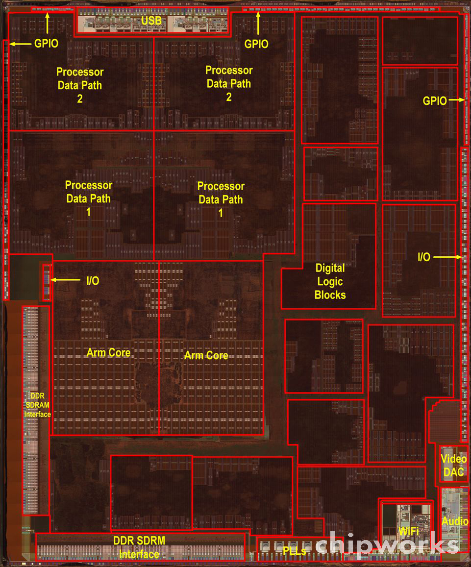
A4:
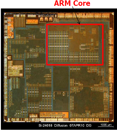
HGi6hzw.png

[10]
  • Manufacturer - Samsung on 45nm process (as featured in iPhone 4)
  • Die Size - 53 mm2 [5]
  • Designer - Apple (Intrinsity[3], also featured in Samsung's 'Hummingbird' SoC[4])
  • CPU Type - 800MHz Cortex-A8 Core with customizations
  • Core Count - 2
  • Instruction Set - ARMv7
  • Chip Designator - S5L8930X
  • L1 Cache - 32/32KB (Instruction/Data)
  • L2 Cache - 512KB
  • RAM - 256MB LPDDR @ 400 MHz (64 bit interface, PoP)
  • Max Theoretical Memory Bandwidth - 3.2 GB/s [1]
  • GPU Type - Dual Core PowerVR SGX 535 @ 200 MHz
  • GPU Performance - 1.6 GFlops, 14 MTriangles/s [2]
A5
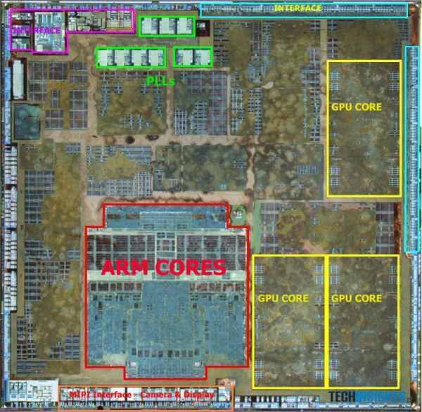
A5:
a5_floorplan_large.jpg

[9]
  • Manufacturer - Samsung on 45nm process (as featured in iPhone 4S)
  • Die Size - 122.2 mm2
  • Designer - Apple
  • CPU Type - 800MHz Cortex-A9 Core with customizations
  • Core Count - 2
  • Chip Designator - S5L8940X
  • L1 Cache - 32/32KB (Instruction/Data)
  • L2 Cache - 1MB
  • RAM - 512MB LPDDR2 @ 800 MHz (64 bit interface, PoP)
  • Max Theoretical Memory Bandwidth - 6.4 GB/s [1]
  • GPU Type - Dual Core PowerVR SGX 543 @ 200 MHz
  • GPU Performance - 14.4 GFlops, 70 MTriangles/s [2]
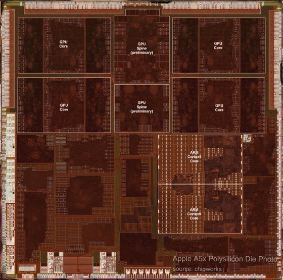
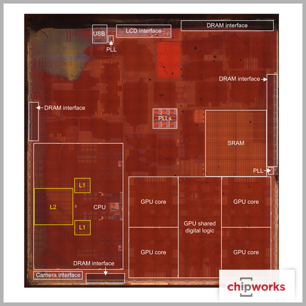
A5X:
apple-a5x-scaled-21.jpg

[8]
  • Manufacturer - Samsung on 45nm process (as featured in 3rd generation iPad)
  • Die Size - 165 mm2
  • Designer - Apple
  • CPU Type - 1GHz Cortex-A9 Core with customizations
  • Core Count - 2
  • Instruction Set - ARMv7
  • Chip Designator - S5L8945X
  • L1 Cache - 32/32KB (Instruction/Data)
  • L2 Cache - 1MB
  • RAM - 512GB LPDDR2 @ 800 MHz (128 bit interface, off package)
  • Max Theoretical Memory Bandwidth - 12.8 GB/s [1]
  • GPU Type - Quad Core PowerVR SGX 543 @ 250 MHz
  • GPU Performance - 36 GFlops, 175 MTriangles/s [2]
A6
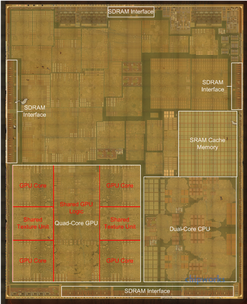
A6:
Apple%20A6%20Die%20diffusion-marked-2%20pass_575px.jpg

[7]
  • Manufacturer - Samsung on HKMG 32nm process
  • Die Size - 96.71 mm2
  • Designer - Apple
  • CPU Type - 1.3GHz "Swift" Core
  • Core Count - 2
  • Instruction Set - ARMv7s
  • Chip Designator - S5L8950X
  • L1 Cache - 32/32KB (Instruction/Data)
  • L2 Cache - 1MB
  • RAM - 1GB LPDDR2 @ 1066 MHz (64 bit interface, PoP)
  • Max Theoretical Memory Bandwidth - 8.5 GB/s [1]
  • GPU Type - Triple Core PowerVR SGX 543 @ 325 MHz
  • GPU Performance - 36 GFlops, 175 MTriangles/s [2]
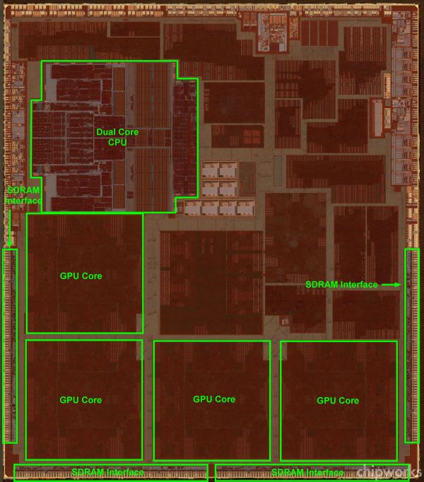
A6X:
a6x_575px.jpg

[6]
  • Manufacturer - Samsung on HKMG 32nm process
  • Die Size - 123 mm2
  • Designer - Apple
  • CPU Type - 1.4GHz "Swift" Core
  • Core Count - 2
  • Instruction Set - ARMv7s
  • Chip Designator - S5L8955X
  • L1 Cache - 32/32KB (Instruction/Data)
  • L2 Cache - 1MB
  • RAM - 1GB LPDDR2 @ 1066 MHz (128 bit interface, off package)
  • Max Theoretical Memory Bandwidth - 17 GB/s [1]
  • GPU Type - Quad Core PowerVR SGX 544 @ 300 MHz
  • GPU Performance - 86.4 GFlops, 210 MTriangles/s [2]
A7
A7:
A7.jpg

[8]
  • Manufacturer - Samsung on HKMG 28nm process
  • Die Size - 102 mm2
  • Transistors - Approximately 1 billion
  • Designer - Apple
  • CPU Type - 1.3GHz "Cyclone" 64-bit Core (1.4GHz for iPad products)
  • Core Count - 2
  • Instruction Set - ARMv8-A (with custom Apple extensions)
  • Chip Designator - S5L8960X
  • L1 Cache - 64/64KB (Instruction/Data)
  • L2 Cache - 1MB
  • L3 Cache - 4MB
  • RAM - 1GB LPDDR3 @ 1600 MHz (64 bit interface, PoP for iPhone)[13][14]
  • Max Theoretical Memory Bandwidth - 12.8 GB/s
  • GPU Type - "Quad Cluster" PowerVR 6430 @ 450 MHz[15]
  • GPU Performance - 73.9/110.8 GFlops (FP32/FP16)
A8
A8:
APL1011_TMET05_166628_Poly_blog_blocks.png

[16]
  • Manufacturer - TSMC on HKMG 20nm process
  • Die Size - 89 mm2
  • Transistors - Approximately 2 billion
  • Designer - Apple
  • CPU Type - 1.4GHz "Typhoon" 64-bit Core
  • Core Count - 2
  • Instruction Set - ARMv8-A (with custom Apple extensions)
  • Chip Designator - APL1011
  • L1 Cache - 64/64KB (Instruction/Data)
  • L2 Cache - 1MB
  • L3 Cache - 4MB
  • RAM - 1GB LPDDR3 @ 1600 MHz (64 bit interface, PoP for iPhone)[14]
  • Max Theoretical Memory Bandwidth - 12.8 GB/s
  • GPU Type - "Quad Cluster" PowerVR GX6450 @ 450 MHz
  • GPU Performance - 73.9/147.8 GFlops (FP32/FP16)
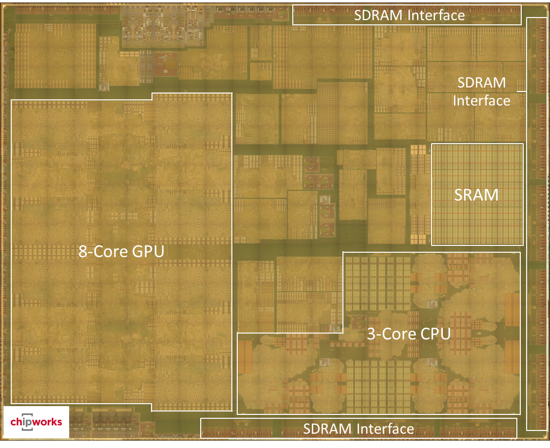
A8X
A8X:
A8X%20draft%20floorplan.png

[17]
  • Manufacturer - TSMC on HKMG 20nm process
  • Die Size - 128 mm2
  • Transistors - Approximately 3 billion
  • Designer - Apple
  • CPU Type - 1.5GHz "Typhoon" 64-bit Core
  • Core Count - 3
  • Instruction Set - ARMv8-A (with custom Apple extensions)
  • Chip Designator - APL1012
  • L1 Cache - 64/64KB (Instruction/Data)
  • L2 Cache - 2MB
  • L3 Cache - 4MB
  • RAM - 2GB LPDDR3 @ 1600 MHz (128 bit interface, PoP for iPhone)[14]
  • Max Theoretical Memory Bandwidth - 25.6 GB/s
  • GPU Type - "Octo Cluster" PowerVR GX6850 @ 450 MHz
  • GPU Performance - 147.8/295.6 GFlops (FP32/FP16)
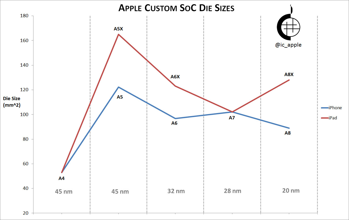
Apple SoC die sizes:
F8kMAHF.png


Apple SoC family attributes:
edPXIlE.png


A9 Prediction
A9
  • Manufacturer - Samsung on 14nm 14LPE FinFET process*
  • Die Size - 100-110 mm2
  • Designer - Apple
  • CPU Type - 1.4GHz Fourth Generation Custom Apple Core
  • Core Count - 2
  • Instruction Set - ARMv8-A (with custom Apple extensions)
  • L1 Cache - 64/64KB
  • L2 Cache - 1MB
  • L3 Cache - 8MB
  • RAM - 2GB LPDDR4 @ 1600 MHz (64 bit interface, PoP for iPhone)
  • Max Theoretical Memory Bandwidth - 12.8 GB/s
  • GPU Type - "Quad Cluster" PowerVR GT7400 @ 450 MHz
  • GPU Performance - 73.9/147.8 GFlops (FP32/FP16)
A9X
  • Manufacturer - Samsung on 14nm 14LPE FinFET process*
  • Die Size - 120-130 mm2
  • Designer - Apple
  • CPU Type - 1.5GHz Fourth Generation Custom Apple Core
  • Core Count - 3
  • Instruction Set - ARMv8-A (with custom Apple extensions)
  • L1 Cache - 64/64KB
  • L2 Cache - 2MB
  • L3 Cache - 8MB
  • RAM - 2GB LPDDR4 @ 1600 MHz (128 bit interface)
  • Max Theoretical Memory Bandwidth - 25.6 GB/s
  • GPU Type - "Octo Cluster" PowerVR GT7800 @ 450 MHz
  • GPU Performance - 147.8/295.6 GFlops (FP32/FP16)
* While Samsung (and TSMC) refer to their FinFET processes as 14nm or 16nm, their metal interconnect technology is re-used from the 20nm node, so the density increase will not be as great as it would normally be for a node transition.

The purpose of this piece is to preview and predict the features of the iPhone 6S (and related iPads). If you have not read MacRumors rumor roundup, please go do so before reading this.

A Look Back to Last Year
This will mark the third year I've done an Apple SoC and device preview. I did an A7 prediction thread two years ago, and an A8 prediction last year, both of which you can find linked in the more reading section. For the A7, the prediction proved to be almost exactly on for the GPU, just narrowly missing on operating frequency but getting the configuration correct. It also correctly predicted the foundry and process, though that was not hard with the strength of the rumors suggesting Samsung's 28nm process. It also predicted the RAM type (LPDDR3) and size (1GB), but missed on frequency (1333 vs. 1600 MHz).

The A8 prediction was very close on the CPU, but missed significantly on the GPU, as the device ended up featuring four GPU "clusters" again instead of the predicted six. A major miss was the amount of RAM predicted. Prior to the A8 and iPhone 6, at least every other generation of iPhone had seen an increase in RAM capacity. The 10% shrink in die size compared to the A7 was also quite unexpected, especially given that the die roughly doubled in total number of transistors.

The post also accurately predicted the cellular radio and transceiver, which was greatly assisted by leaked PCBs that showed the 9625M modem. The modem necessitated the presence of the companion WTR1625 and WFR1620 chips, which were also located. PCB analysis also revealed the QFE1100 envelope tracker for dynamic RF chain power adjustment. The WiFi footprint had grown relative to previous generations, and the existence of an integrated Broadcom solution for wireless AC made it clear that a solution featuring the AC standard was likely.

Display
The display was predicted to change, in line with the strong rumors of both 4.7 inch and 5.5 inch displays. No quality improvements were predicted, mostly based on the fact that no rumors or analysis of leaks led us to believe the displays would be anything but a shift in size from the 4 inch screen, which had already improved color gamut and adopted in-cell touch assemblies over the original retina display. Apple made it a point to mention specific improvements to the display in their keynote, a primary example being dual domain pixels for improved color distortion performance on off-angles. Anandtech and DisplayMates's reviews of the iPhone 6 and 6 Plus displays revealed improved contrast, color accuracy and off-angle performance. To summarize, it was the best LCD display ever featured in a phone.

The use of sapphire over gorilla glass for the display was perhaps the hottest talking point surrounding the new iPhone's development, which was already a staple of the iPhones' camera lenses. There was much debate over whether they would be included, despite the strength of the rumors regarding their development. It was eventually revealed that gorilla glass was again in use, which made sense given the ultimate resolution of Apple's bankruptcy settlement with sapphire producer GT Advanced. It seems clear that Apple intended to use sapphire in their displays, but the plans succumbed to poor management at GT Advanced.

Flash Storage
NAND storage was an interesting topic because of schematic leaks that showed 16GB, 64GB and 128GB storage options, making for an easy prediction. This matched with flash makers' announcements of NAND densities sufficient to reach 128GB modules with eight die inside a single package. The confusing part of the schematic rumors definitely centered around a 1GB flash module, which was briefly mistaken for RAM. This 1GB NAND was never located on the board or inside the application processor package, so if the leak was legitimate, it would need to be housed inside the flash memory package with the other die. As to its purpose, I suggested at the time that it could be related to secure storage of fingerprint or health data. Given that this 1GB pool was never confirmed to exist, we'll have to relegate it to rumor once again.

Battery
Thanks to increased chassis size due to larger displays, larger capacity batteries seemed a given - a desire that had been in constant war with Apple's quest for thinner devices. There were several leaks featuring potential batteries for the new iPhones that turned out to be accurate. The iPhone 6 had 1810 mAh and 2100 mAh capacities rumored, whereas the iPhone 6 Plus had 2915 mAh. The smaller size turned out to be accurate for the iPhone 6, while the only 6 Plus leak was also accurate. Apple changed battery chemistry at the time of the iPhone 5 with much of the rest of the industry. The new chemistry allowed for more efficient discharge and perhaps enhanced battery lifetime, and there hasn't been any interesting battery rumors to cover since that point outside of capacity size.

CPU
CPU architecture is an area in which Apple had made tremendous strides in successive years prior to last year's A8. A6 was Apple's first full custom design, which was followed by an industry first 64-bit A7. The year over year 2x performance improvement from each of these was made possible by ISA and process technology advancements, along with a very generous helping of engineering talent. Last year, Apple had a full node transition from 28nm to 20nm at their disposal, but my CPU prediction was very muted based on the strength of the A7 design.

Apple's A7 was a huge advancement in mobile CPU architecture. With an issue width of six micro-ops, Apple was rivaling desktop processors. Nvidia's custom 64 bit core does have an issue width of seven, but we're likely reaching the practical limits of issue width for today's workloads. Skylake, Intel's latest microarchitecture, also features a dispatch of six micro-ops per cycle. A handful of smaller optimizations to the architecture were predicted, including things like improved ALUs, an improved memory architecture, and reduced latency for complex ALU operations. All of those improvements came to light through Anandtech's benchmarking in their A8 review. Apple also seems to have moved to independent L2 cache designs for each core, as noted by Chipworks. This makes sense, as the L3 last level cache is still shared.

One focus Apple emphasized was sustained performance on A8. Although performance gains were only up to 20% in most cases, they wanted to reduce the throttling becoming more common in mobile processors as thermal limits were reached. As Anandtech's review shows, they definitely achieved this goal. The review remarked how it was the first processor to be put through the benchmark suites that did not throttle during performance tests. This is pretty significant, as mobile SoC makers had been progressively pushing for more peak performance to advertise the gains for which consumers had developed an appetite.

GPU
The GPU prediction from last year had two main components, the first of which was another architecture upgrade. The A7 saw Apple adopt Imagination Technologies' "Rogue" Series 6 architecture just a little over a year after its announcement. In early 2014, ImgTec announced the XT series addition to the Rogue family. It had features like ATSC compression support, as well as finer DVFS options, dubbed 'PowerGear'. The XT series also increased FP16 throughput by 33%, effectively making it double that of the FP32 throughput. While FP16 vs. FP32 usefulness on mobile is a debate of its own, to end result was Apple claiming up to 50% speed improvements. Most benchmarks showed modest gains, with some cases pushing towards the 50% theoretical improvement.

The second reason a six cluster GPU was predicted was the full node transition from 28nm to 20nm. With mild changes to the CPU predicted, there would be plenty of extra transistors for GPU increases if the die size stayed relatively constant. Apple had also pushed GPU performance quite hard generation after generation. It turns out that transistor growth for a given cluster count increases quite dramatically going from the G6x30 series GPUs to their GX6x50 successors. In what could theoretically be a 50% increase in transistor density thanks to a whole node shift, the GPU only shrunk about 10% from A7 to A8. It's clear that the extra ALUs, compression hardware, and cluster power control circuits have a hefty transistor overhead.

RAM
The stalemate on application processor RAM was somewhat of a surprise. Prior to the iPhone 6 and 6 Plus, the iPhone had doubled RAM at least every other generation. We did see the iPad Air 2 gain 2GB of RAM with the A8X, but that move was to help support the split-screen multi-tasking of the full size iPad. Also, while there had been rumors of Apple adopting LPDDR4 for the A8, it seemed too early in the memory's product lifecycle for sufficient volume to be available to Apple, resulting in LPDDR3 being used again.

Regarding RAM, I'd like to call back to the A7 design when Chipworks examined the package. There was a large increase in pads, which suggested that we would see an 128 bit memory interface rather than the 64 bit memory interface that had become common on Apple processors. This large padout was again seen on the A8 package, and we still have no answer for the increased number of pads, as those processors feature 64-bit memory interfaces. Perhaps Chipworks has since discovered the answer and keeps it in one of their paid reports, but it's an interesting development to keep in the back of your mind as we move forward.

Audio
Device audio is another area of small but keen interest for some. Android has recently seen some adoption of 24-bit audio to cater to audiophiles, and suggestions that Apple would require artists to submit 24-bit masters to iTunes stoked the flames for some. Anandtech covers audio performance pretty well in their A8 review, giving the audio codec praise for its harmonic distortion and noise performance. This seems to be an area where we may see some activity, as some think there are some obvious gains to be had by improving audio bit depth.

Rather than enhancing the DAC or amplifier stages of the audio chain, I also theorized that Apple could leverage their MFi program to create hardware through their recently acquired Beats brand that featured built-in DACs and/or amps to market to the audiophile segment. This possibility did turn out to be a reality, but via third party Philips.

A8X
Last year, we also saw the re-introduction of an iPad specific processor via the A8X. After the A7 remained the only application processor design for the iPhone 5S, iPad Air, and Retina iPad mini, many had assumed that Apple had now deemed GPU performance sufficient for one SoC to power all the iDevices released in a given year. A8X proved that wrong, with a GPU double the size, a third CPU core, double the L2 cache, and double the RAM. The new multitasking features in iOS served as an impetus to have a high performance tablet version of the A8 SoC. In retrospect, the design effort that the A7 represented could be the reason it existed as the sole processor product of Apple that year. Apple was devising a huge architecture shift on a very new ISA in addition to a new GPU architecture adoption, so all design resources may have been required to hit their target goals. With the more modest architecture changes on A8, they could devote resources to developing the A8X on a similar timeframe.

One last thing to mention about the A8X is what the die shot shows. We know from diagnostics that the CPU cores have 2MB cache. If you grab the L2 cache from the A8 shot, you can superimpose it and see that there clearly appear to be blocks two times the size of the A8 L2 cache. However, there's only two of them despite there being three cores. What's going on there, an asymmetric cache structure where two cores share an L2? That seems unlikely and I'm probably missing something obvious, but it's an interesting difference to point out.

Fixed Function Blocks
I have saved the most interesting part of the A8 for last, and that centers around transistor density and die size. As soon as Apple announced the transistor count had approximately doubled from the A7 to A8, I began to imagine ways they could have incurred such transistor growth. An obvious candidate would have been the aforementioned predicted GPU size increase. SRAM size increase would be another obvious one, as their six transistor bit structures are easy ways to push up transistor count while also being very dense. That didn't turn out to be true, either, with L1, L2 and L3 caches all staying the same size.

The GPU did see its transistor budget increase quite a bit, but not by a considerably large amount, while the CPU increases were very minimal. This turns us to fixed function blocks. Apple's efforts in fixed function and mixed signal blocks has been an area of interest for some time. From the keynote, we know two significant fixed function blocks that would cause transistor growth. The first was a change to the ISP that allowed for 240 fps slo-mo video, doubling the previous 120 fps slo-mo. The second was what Apple referred to as a "desktop class" image scaler. With the introduction of the iPhone 6 and 6 Plus, graphical elements were no longer necessarily neat multiples of one another across generations, so Apple allowed the iPhone to downsample graphics drawn at a higher resolution to preserve nice pixel multiples.

These fixed function additions don't tell the whole story, but they begin to explain how Apple could have such large GPU growth without significantly increasing the main sources of transistors: GPU, CPU and SRAM. What is also very interesting is that the transistor density scaling they achieved. From an absolute ideal standpoint, a given design could scale to approximately half of its size on a full node shrink. However, not all circuit types scale the same way, and transistors don't always scale the same way in channel width as they do in length. Realistically, you are then looking at probably 70% scaling. However, going from 1 billion to 2 billion transistors (and perhaps rounding is on Apple's side here) means Apple is looking at a near 0.45 scale factor. With SRAM/cache being the best bet for increased transistor density, they did not change at all in memory capacity yet Apple achieved this scaling factor. Once again, Apple has some extremely talented engineers.

What You Should Have Read This Past Year
In this section, I'd like to highlight some reading from the past year that provides context for the state of the industry and technology at this time.

Anandtech's iPhone 6 Review - Anandtech continues to put out the best iDevice reviews even after losing Shimpi and Klug to Apple. They are the reason we have many of the microarchitecture details on Apple's custom SoCs.
Anandtech's iPad Air 2 Review - In addition to the above, this gives us a look at the A8X.
Displaymate iPhone 6 and 6 Plus Display Review - A critical look at display performance on the iPhones released last year.
Enhanced Sapphire - DisplayMate gives a short technology overview of a new type of Sapphire that beats glass in reflectance tests, which means better ambient light performance. All while still being more scratch resistant than glass.
Thin Loop Heat Pipe - Fujitsu has developed a heat pipe that dramatically improves cooling performance in a form factor suitable for phones. This isn't just about being able to use more power in a given thermal envelope. Lowering heat for normal CPU operations lowers leakage current due to heat and can have other benefits.
Light-splitting camera patent - Apple patented a system for splitting light into its individual color components to enhance image quality. They adapted a technology often seen in larger video capture devices to a mobile form factor.
Tile-based rendering overview - ImgTec explains how their graphics processors work using tile-based rendering. It's a proven power efficient rendering method, which is why it has found such a good home in mobile spaces.
Apple Watch System-In-Package - A great short blog entry that covers the packaging advance that the Apple Watch represents.
Semiconductors from idea to product - A great overview of the flow of semiconductor IP from idea to real silicon. Gives a great context to understanding feasibility and time-to-market concerning rumors.
An Introduction to Semiconductor Physics, Technology, and Industry - Great companion read to the link above. Gives a broad but detailed overview of the state of semiconductors, process flows, and challenges faced by the IC industry. If you only read two links, make it these two.
Inside ARM's Cortex-A72 microarchitecture - a dive into ARM's latest high performance 64 bit reference core. This will power many of the rival smartphones Apple will face and will serve as one of the comparison points in benchmarks.
A comparison of HBM, Wide IO, and Hybrid Memory Cube - an overview and comparison of the 2.5D and 3D memory technologies that will eventually take over for LPDDR memory in mobile devices.
Avago purchase of Broadcom - Avago and Broadcom both have IP in several generations of the iPhone. The acquisition could have implications for Apple and the industry as a whole.
Teardown of the iPhone 6 Plus battery - Nice overview of today's battery technology with a cost analysis thrown in.
Comparing OpenGL ES To Metal - A benchmark comparison of the standard OpenGL ES and Apple's proprietary metal drivers.
The IP licensing model - A follow-on to the IP development process from another ImgTec engineer. It covers the relationship between device IP licenser and licensee.
Understanding Qualcomm's Snapdragon 810 - While it covers the entire Qualcomm Snapdragon solution, the sections on the RF components are good, especially since the next iPhone will use some of them.
Understanding Qualcomm's ImproveTouch - On the eve of Force Touch displays, it's important to understand the competitors' technologies and solutions.
Galaxy Note 5 Display Shootout - Samsung now makes the best reviewed smartphone displays, so they are the benchmark for Apple.
Hunting Down a Turncoat - A very well written account of the former TSMC executive who became disenchanted with his employer over a skipped promotion and eventually gave his company's technology process secrets to Samsung.
 
Last edited:
The Prediction
These predictions are based on a mixture of supply chain rumors, historical cadence in Apple's SoC offerings and inference based on what parts are available on the market that would make sense for Apple's likely goals.

SoC
CPU
Comments on Typhoon
In this section last year, I had a lot of thoughts to convey about Cyclone even though I had already covered it in the look back on last year. The shift to a custom 64-bit core blindsided consumers and competition alike. I still fondly remember the Anandtech live blog typing 64 bit with likely more exclamation marks than had previously been published on the site as a whole. After two years, Apple's competitors are finally hitting the market with their own custom 64 bit ARM cores. Only Nvidia has yet to ship a device with one besides Apple.

After Cyclone, it was time to come back down to earth. Apple had approached or matched the features of some of the leading desktop processors at the time, so A8 was bound to be an evolutionary change. Indeed, we saw memory hierarchy improvements and incremental ALU improvements and reductions in latency. The CPU is roughly 10 to 20 percent faster than its predecessor, which is a typical IPC improvement we'd see out of an Intel processor revision. We're probably looking at a new normal.

The A9 CPU prediction
When talking about Apple's CPU efforts, it's important to remember how they got to the capability level that they are at now. Acquiring Intrinsity, PA Semi, among others, and hiring top CPU architects from AMD shows how serious Apple is about top performing, custom CPU solutions. Apple also turned heads with their Macroscalar trademark three years ago, but it is unclear whether any technology related to this has come to market or why Apple felt the need to trademark what would likely be considered a trade secret design process. Moreover, all speculation about the trademark seems to come back to established methods of branch prediction and speculative execution. It will be interesting to see if this topic comes up again at all.

Before I begin the CPU prediction, I'd like to preface it with a discussion on die size and transistor density increase. From the leaked PCBs, we can see that the A9 package has grown about 10.5% from the A8 package. If we assume the die has scaled accordingly, we arrive at a die about 98 mm^2, which is 4 mm^2 shy of the A7 die.

Scaling transistor density is a little more difficult. If predictions and rumors hold true, Apple will have gone from Samsung to TSMC and back to Samsung for the past three generations. I believe we can assume that Samsung and TSMC transistor densities were quite similar at the 28nm and 20nm nodes, especially given Samsung poached a key technology executive from TSMC and analysis has revealed the processes are very similar. This is outlined in the 'To Catch a Turncoat' piece in the reading section above. TSMC claims that their 20nm process allows for up to 1.9 times the density of their 28nm process, whereas Samsung claims their 14nm FinFET process allows for 50% area scaling from their 28nm process. The difference only accounts for about a 2.6% scale from 20nm to 14nm (or 16nm) FinFET.

TSMC, for their part, was engaged in a public spat with Intel about their technology scaling, in which they claimed that their FinFET process had a 15% scaling factor over their 20nm planar process. Their reasoning that transistors can get smaller and have the same drive capability is fairly intuitive given FinFET transistors' ability to form a channel easier is part of the reason they exist. Therefore, it seems fair to ascribe some non-negligible scaling factor even though we don't have statements from Samsung on scaling from 20nm planar to their own 14nm FinFET. Now that we're all caught up, 14/16nm FinFET processes actually use the same metal interconnect technology from the 20nm planar node. Thus, if metal interconnect pitch is driving the size of your circuit rather than the size of FETs as it often does, you won't see much scaling from 20nm.

Given that Apple has a very talented team of engineers, they can likely meet or beat any normal scaling between processes, so in total with a 10.5% die increase and transistor scaling at somewhere around 10% or less, we arrive with a transistor budget roughly 20% greater, or 400 million transistors from A8. We know from A8X transistor counts that four series XT graphics cores, 4MB of total extra L2 cache, and one Typhoon CPU core total roughly one billion transistors, so this number would afford some considerable circuitry, but not a huge overhaul. We should also keep in mind we're dealing with a large margin of error on this scaling factor, possibly as big as +/- 10%.

With a budget of 400 million transistors, Apple could increase each L2 cache to 2MB to match the A8X and bump the L3 cache up to 8MB while still having roughly 100 million transistors left. Some competing designs already have 2MB L2 caches in phone form factors. Although, if that were to occur, the L3 would need to increase to 8MB by necessity since successive cache layer ratios are usually 4:1 or greater, with A8X being a curious exception. Alternatively, they could probably add a third CPU core with all else constant to bring it up to par with A8X. Of course, they could also devote the majority of this transistor budget to the GPU or fixed function blocks, which we'll cover later. Given the third CPU core seems to have been added to the A8X to address unique multitasking usage models which do not occur on an iPhone, a third CPU core seems an unlikely candidate. Outside of CPU microarchitecture changes, the most likely source of transistor growth in that area would be L3 cache growth to 8MB. I will touch on the importance of that later. Given the usage model of the iPad Air 2 and A8X, the move to 2MB L2 cache may have been to help multitasking, so I wouldn't consider it a sure thing for the A9.

Before we move on from foundry process technology, it's important to mention that Samsung has two 14nm process offerings. Their Low Power Early (LPE) offering is what is seen in their own Exynos 7420 SoC launched this Spring. Low Power Performance boasts 10% greater performance, but seems to be focused on volume shipments in 2016. Therefore, Apple seems likely to go with the former given the time frame and their high volume requirements.

As for direct CPU core changes, we shouldn't expect too much. Apple has quickly forced themselves to the rather flat part of the diminishing returns curve when it comes to extracting parallelism from their execution flows. Further improvements are likely to minor and similar to the type of gains that we see Intel make. Examples would be reducing latency on a complex floating point operation, increasing the accuracy of a branch predictor, or lengthening a re-order buffer to further prevent pipeline stalls. There is still reason for optimism, as Apple has gleefully plowed through any perceived limits on their acumen for surprising us with their accomplishments. A8's processing gains were modest, but its ability to function at peak performance relatively indefinitely set Apple apart from the field once again.

It's also important to stress that this necessarily has to be yet another minor performance gain as A8. FinFETs are great performing transistors, and Samsung claims a 35% power savings with the same performance compared to 20nm, or alternatively, 20% more performance in the same power envelope. Apple seems to have largely got their power consumption issues under control, so it seems some performance gains would be in order for A9. It may also be a good reason to not be too concerned about the rumors of a slightly smaller battery capacity this generation. Still, I would expect a relatively minor CPU frequency boost of no more than 100 MHz if one occurs at all. There is precedent for one not occurring at all, as was seen in the A4 to A5 transition and the A6 to A7 transition.

CPU core speed is an important point too, because Apple has typically lagged well behind the industry for high-end SoCs. Many of those are now North of 2 GHz. I explained power in clocked devices last year, where a circuit's power is some multiple of its frequency of operation, it's average load capacitance, and the square of its applied voltage. Since the frequency you can operate at is directly tied to your applied voltage, it will necessarily go lower as you target voltage to get your circuit power down. Recently at IDF, an Intel architect claimed that relationship is closer to being proportional to the cube of your applied voltage. It suffices to say that transistor models necessarily become more complex to maintain accuracy as the feature sizes get smaller, making applied voltage even more critical. To put it simply, Apple's lower clock frequencies allow them to get comparable battery life to competing smartphones with significantly less battery capacity.

Last year I spent a while on the concepts of Apple's position in the market in terms of core design, their rapid design iteration owing itself to quick ISA steps, and some overall comments on core counts in the industry. That October, over a year from the debut of the A7, the mobile industry got its second custom 64 bit core with Nvidia's K1 "Project Denver" design. That core had an issue width of seven, stealing Apple's crown in the process. It executes ARM code through a binary translation process though, so it's an interesting topic to read into by itself.

While competitors seemed to be gravitating back to two core designs with the ability to dispatch a lot of operations per cycle, many core designs are still holding strong with Samsung, as well as big.LITTLE core configurations. All of the custom players adopting the former likely points to it still being the clear optimal solution in this case.

The ISA advances, and reference core advances are now merely keeping up with Apple rather than helping them push the envelope. ARM's new A72 microarchitecture was revealed this year, but much of its attributes, down to the identical pipeline length, make it appear as a contemporary of the A8 design rather than a clear successor. It will certainly be interesting to see phones featuring those cores pop up in benchmarks next year to see how the cores compare.

ARM also introduced a revision to the ARMv8-A ISA, ARMv8.1. The improvements include some SIMD instruction enhancements, several atomic operations, some security enhancements, and finally some performance profiling additions. Given Apple's focus on security, it would seem the protected state alone could be enough to attract them to adopting these enhancements. Given the time of this disclosure, its inclusion in A9 seems unlikely given how early architecture decisions are locked down, but Apple has made a habit of surprising us here in the past. The other improvements have potential for modest gains overall.

GPU
All versions of the iPhone have featured a GPU from Imagination Technologies. In fact, Apple owns around a 10% stake in them as well (an interesting side note- ImgTec acquired Caustic Graphics, a company focused on creating dedicated ray tracing hardware that was comprised of former Apple engineers). It seems all but certain that Apple's A9 will feature ImgTec graphics core as well, with Imagination Technologies announcing a multi-year, multi-use extension to their licensing agreement with Apple. Last year, ImgTec's Series 6 "Rogue" architecture had previously been seen in the A7 design, and we were eying the 'XT' evolution for inclusion in the A8. Despite the fast time to market from announcement, the A8 included that XT variant. Now we find ourselves again at a new numbered series transition, which ImgTec has said they want to make a habit.

One positive thing about the GPU landscape is that ImgTec has been very good about publishing data on their architectures over the course of the past several years. The PR package they delivered to tech websites is quite a good overview, and Anandtech has a good take. The first point to be clear on is that while the new GPUs are called Series 7, they are very much "Rogue" designs at heart with a lot of optimizations, rather than paradigm shifts similar to what we saw from Series 5 to Series 6. Given that the architecture was publicly disclosed last November, odds seem good that this GPU will be featured in Apple's A9.

You can read the article to get a detailed explanation of the improvements, but they boil down to better efficiency, throughput, and improved scheduling. The essentials of peak FP16/FP32 throughput are unchanged, so this architecture will earn its keep by doing things more power efficiently and getting closer to its theoretical maximum performance. The XT series seems a given, and it has optional components which feature FP64 and D3D11 support as features. As for FP64, double-precision is something we see in compute environments, so that will very likely not be included. As for D3D11 support, there's no reason to support a Windows graphics API, but that does not preclude Apple from potentially exposing any functionality with Metal, though that seems a very unlikely election.

Performance in common graphics benchmarks is listed anywhere from a 30% to 60% improvement, so Apple could seemingly adopt the four cluster 7 series XT variant with the same clock speed used in the A8 and automatically get those gains. That may be an attractive incremental option if there are other areas that are more important to spend our theoretical 400 million transistor budget increase.

A key element of the upgrade discussion for the GPU, as well as the CPU and ISP, is the fact that the L3 cache is shared among all of them. Thus, all stand to benefit from an increase to 8MB for L3 cache. GPUs can almost always utilize more memory bandwidth, and with the rumor of 4K video capture, the ISP's data throughput demands are only going to increase as well. At this point, the trade for those transistors seems to be between the GPU and the SRAM, as the ISP likely needs to grow regardless. Given the shared benefit of the L3, it seems slightly more likely to expect a cache increase with the GPU remaining at four clusters rather than increasing to six (ImgTec has confirmed odd cluster arrangements are not possible, for those curious).

As for future GPU architecture direction, Beyond3D forum user tangey dug up an interesting patent application from Apple regarding disabling high power GPUs. The patent details a way for the system to monitor GPU throughput demand and dynamically disable or enable to high power GPU to swap duties with a smaller, low power GPU. Given most situations have light graphics processing demand outside of games, the appeal of such a solution is clear for power saving measures. While it does not seem a guaranteed thing for future SoCs, it is an area future teardowns should pay attention to.

Two years ago, I also addressed Apple's GPU engineer team in Orlando, FL. I suggested it could indicate that they intended to create their own customized versions of ImgTec GPUs, fully custom GPUs, or API/driver improvements to speed things up from the software side. Apple confirmed my last suggestion when they announced the "Metal" (a reference to "coding to the metal", or low level programming that directly addresses the features of the hardware) shader programming language designed to eliminate driver overhead when writing graphics code. Driver overhead can be significant, as well. It is the reason that AMD introduced their own custom graphics API, Mantle. It's also the reason that video game consoles are able to succeed in the face of much more powerful PCs. It is quite possible that my other ideas on this team's function may come to fruition, but this advancement has already shown at least moderate benefits in benchmarks.

It is worth noting that ImgTec has also introduced a variant of the 6 Series GPU that features dedicated ray tracing hardware, which should carry over to Series 7. Ray tracing is a physically based lighting method that is more accurate than traditional rasterization methods but much more computationally expensive and memory intensive. CPUs and even GPUs do not do it well. There have been previous attempts to do it with custom silicon that have also failed. However, ImgTec recently acquired Caustic Graphics who have dedicated hardware solutions, which according to famous graphics programmer John Carmack, are actually quite good. ImgTec decided to integrate it into their Series 6 GPUs, making them the first consumer GPUs with dedicated ray tracing hardware.

The problem with ray tracing hardware is that developers would have to implement support for it to actually be useful. While some applications that render 3D graphics may be able to make use of it, the primary use would likely be games. It is often a tough sell to get developers to put major features into games that only a small subset of users will utilize. This is above and beyond the technical challenges it poses. Indeed, before being disclosed on the Caustic hardware, Carmack stated with 90% certainty that any eventual ray tracing hardware would likely be small modifications to existing GPUs. He also downplayed the need for it all together in modern games. Thus, it is likely to be relegated to a curiosity for at least the next few years.

RAM
This time last year, leaked PCB shots had already given us the product codes from package silk screens to determine that we were again looking at 1GB of LPDDR3 RAM at 1600 MHz. This was surprising because, as you can see from the list of previous iPhones, Apple has never kept the same amount of RAM in the iPhone for more than two generations. Many aspects of their devices have a two year cadence including but not limited to form factor, product naming, screen size and technology, and many other features. This year, we are in the dark, as the PCB leaks we have thus far have no such product codes for us to determine what kind of memory is inside the package.

There had also been a rumor earlier last year that suggested Apple may look to include the new LPDDR4 RAM in their iDevices this year. Part of the rumor was based on a 250 million dollar mystery payment made to Micron (who now own Elpida, memory supplier on previous iPhones). While Apple has been known to make large payments to suppliers in the past in order to secure volume and favorable pricing, it seems that this supposition was perhaps unfounded in this case. A large part of the reason it likely cannot be adopted is because suppliers cannot provide volume or acceptable pricing for Apple's needs. Indeed, the standard for LPDDR4 was just ratified by JEDEC in weeks prior to A8's reveal. That being said, LPDDR4 is a significant improvement over LPDDR3, much more so than LPDDR3 was over LPDDR2. It has a lower voltage and completely new interface that will offer significantly more speed and power savings. Apple will likely look to adopt it as soon as possible given their volume and pricing constraints.

This year, Apple seems much better positioned to adopt LPDDR4 memory, as many of their competitors have done this year. Rumors do seem to be pointing toward 2GB of LPDDR4 for the A9 processor. The bumping of total RAM to 2GB is interesting because of its exclusion last year, making it the third year of 1GB RAM in iPhones. Apple did introduce 2GB RAM with the A8X and iPad Air 2, but the need for this seemed to be largely driven by the iPad's enhanced multi-tasking capabilities, which would necessitate two potentially large programs needing their data in the local RAM at all times. Apple's iPhones have no such usage state, and memory footprints haven't obviously been increased with any new iOS features. It appears that this move would be a simple incremental update that is driven by a combination of potentially obscure factors. Such a change to 2GB memory would no doubt be welcome, as application data being forced out of main memory due to multitasking is a common complaint amongst iOS users, even given memory compression has been in use since iOS 7.

With A9, we should keep Chipworks' analysis of the A7 in mind as it revealed that the memory package had decreased its pad pitch and increased the number of pads from 272 in the A6 to 456 in the A7. This was repeated again in the A8 and there still hasn't been a technical explanation for these changes.

Looking into the future, it is likely that we will eventually see 3D IC memory solutions from Apple for their SoCs. Rather than having individual wires interface to solder bumps from the memory chip to the interconnects, 3D IC solutions allow the memory to directly interconnect to the SoC through a silicon substrate by what are called through silicon vias (TSV). This will allow for greatly expanded memory interfaces that are 512 or even 1024 bits wide in comparison to the 64 and 128 bit interfaces currently seen in the iPhone and iPad. Sony uses a predecessor to this technique called System in Package (SiP) that uses fine wires as opposed to solder bumps, allowing them to achieve more interconnects in a given space. This allows the Vita's GPU to have a 512 bit interface to its VRAM.

There are several solutions that fall under the 3D IC hood such as Wide IO, HBM and Hybrid Memory Cube as outlined in the reading section above. All have varying degrees of cost, process complexity, efficiency gains, and performance gains. This presentation highlights a lot of the limits mobile SoCs face with today's solutions and some of the challenges that new solutions face. There are significant gains to be had in all metrics, but there are also significant challenges in terms of cost and scalability for a company like Apple with very sharp demand curves.

Fixed function blocks
Last year, Apple surprised people when they announced that the transistor count had doubled from the approximately one billion transistors on A7 from the year before. The A8 ended up being around 10% smaller in die area as well. Even with the help of a full node transition, Apple beat the most optimistic scaling factor between processes by about 5%. We know the GPU gained a fair amount of transistors for adopting a variant of the Series 6 GPU in the A7. The CPU shrunk quite a bit from a die area standpoint, as it was mostly a minor revision of the A7. The L3 cache stayed the same size at 4MB, so that left a lot of questions as to what functionality was eating up a lot of those transistors.

Apple's keynote actually answered some of the major questions regarding these transistors. The major change was the introduction of a "desktop class" graphics scaler that allowed graphical elements to be rendered at a different resolution than the actual display resolution. The change was the addition of even higher FPS slo-mo video. They essentially doubled the data demand on this block, and it had to grow as a result. With rumors of 4K video at 60 fps being added this year, that demand would only increase and necessitate a larger ISP still. Given that the L3 cache services the ISP, it's also a reason I believe the cache could grow as well.

This is not to say that these are the only two blocks that account for most of the transistor budget increase. There are likely many more functions that grew or were added that we don't know about. In general, adding fixed function blocks this to the application processor is a win. It saves PCB space, simplifies the number of interfaces to the PCB from the SoC and can have performance benefits. In the past, I have talked about Apple's acquisition of LuxVue and pixelworks, and their attempted acquisition of Renesas, who manufactured display drivers. All of these moves show Apple wanting complete control of the rendering and display pipeline, and with the addition of Force Touch, it becomes even more important.

Apple's graphics pipeline efforts make sense in two ways. First, they care a lot about things like color accuracy, image quality and other things that can be controlled by hardware. Second, the display is the main source of power dissipation in a mobile phone. Thus, it makes sense to find ways to stop draw calls when there is no new information to display, find ways to power down unneeded display circuitry, or to dynamically shift the image attributes based on ambient conditions. Apple is clearly making efforts in all of these avenues so it should be something interesting to watch moving forward.

There have been some interesting articles in the past years on this topic, so I've left the rest of this section for the content I presented last year, unedited.

The EETimes article ([11],[12]) goes into great detail about comparing the size of the CPU cores in the A6 to the A5 for those interested. It also helps to illustrate that the CPU has taken increasingly larger amounts of the overall die area in Apple's A-series SoCs (also true of the GPU).

The die allocation image above shows that the number of digital blocks on the A-series SoCs has been increasing. Indeed, with acquisitions like Anobit and Authentec, Apple is poised to put more and more custom circuitry on the SoC itself, freeing up space on their board and allowing them to tailor the solutions exactly to their performance and power needs. I expect this number to go up over time.

Apple also surprised many last year when it was found out that Audience's EarSmart noise cancellation technology would not be in the iPhone 5. The fact that they developed and completed the IP to Apple's requirements suggests that Apple potentially competed them against their own internal team. If this was the case, Apple may been able to meet its own requirements with an in-house solution, eliminating the need to license the IP from Audience. This is just another example of Apple's aggressive pursuit of solutions that are integrated, custom and internally created.

There was also an interesting analysis that arose after the AppleTV received a new version of the A5 SoC that trimmed the CPU to a single core and significantly reduced the size of the die. This seems to be thanks to some custom analog circuitry redesign, which suggests Apple is also increasing its design expertise there. Similar reductions in future SoCs would allow Apple to make all of their dies smaller, saving money, or use that area for something else, increasing performance without increasing size comparatively. The AppleTV was a good product to make this change on because it allowed them to test out their new circuitry in a relatively low volume part.

Comments on design fabrication process, TDP, and die size
Last year, Apple changed foundry partners and had a SoC manufactured at TSMC for the first time. It was believed that TSMC was ahead of Samsung in 20nm node readiness, and that was one of the main drivers. It was also suggested that it signaled Apple gaining independence over Samsung as a supplier - a move that was perhaps rooted in a bitter legal battle beginning back with Jobs. However, Cook seems to have a history of pragmatic supply chain moves, so I think the reason is very likely the former.

This year, it seems as though Samsung is again the partner of choice, with most rumors at least pointing to them as one of the partners. The possibility of both Samsung and TSMC is something I'll get into later. This time Samsung appears to be ahead of TSMC in 14nm/16nm FinFET node readiness, as is evidenced by their release of the Exynos 7420 SoC in April featuring their FinFET process. It seems to be a pretty safe conclusion that this is the process of choice for Apple and the A9.

As for die size, in the CPU section I explained that the package seems to have grown around 10% from the leaked PCB shots. If the die scales perfectly with that, we are around 98 mm^2, a growth of 9 mm^2 over the A8 , 4 mm^2 shy of the A7, and within 2 mm^2 of the A6. Looking at our die size chart, this appears to be the sweet spot that Apple is settling into. iPhone application processor die sizes will fall in the 90-110 mm^2 range, while their iPad variants will bump up to the 120-130 mm^2 range. There are probably a combination of cost and yield reasons that these sizes make sense for Apple. iPhones have turned out to be much higher volume than iPads, so the latter could afford to have a slightly poorer yield.

TDP is, forgive me, also a hot topic in mobile device discussion. Manufacturers have been pushing their peak power measurements up and up over device generations to get higher peak performance numbers. Apple was no exception, and there were user complaints about heat as well as thermal throttling in Apple's SoCs. For example, the A7 draws over twice the current that A6 does during fixed-point operations, and still nearly double during floating-point operations. Apple sought to change that with the A8. While the processor still got hot, thermal throttling was not observed. This will likely remain a design goal of Apple's moving forward, especially as they try to make phone chassis ever more thinner. It's also the reason that easy 2x performance gains generation over generation are a thing of the past.

One idea that I want to focus on is a persistent rumor that Apple will have some combination of foundries, most commonly TSMC and Samsung, share production of a SoC. It has appeared this generation as well. I want to stress the relative difficulty of this task. First of all, Apple does full custom CPU designs. That puts them in a very small group with companies like Intel, Qualcomm, AMD, IBM and a few others. It is much harder to develop your own circuit libraries and layout your chip using custom layout. Most companies opt for standard libraries suggested by their foundry partners and lay out their chips using automated tools. It produces slower, larger and less optimized designs, but it is much cheaper in terms of schedule and man hours. For most, it's a good enough solution.

It is easy to sympathize with the idea that Apple would want to use two foundries to produce their chips. At the time that they are defining their microarchitecture and refining device models for their transistors, their foundry of choice's guarantee on yields would be much less clear than it will be come production time. However, to prepare to release the same custom chip on two processes adds a large scope of oversight and likely an unavoidable schedule push out. Also, that time of conceptualization is probably around 18 months, which should make anyone call into question a rumor that suggests Apple is switching foundries on the fly within a year of an iPhone's launch date. The team must now conceptualize a design and define performance targets to two different, but similar, processes. Some design characteristics will inevitably take on a lowest common denominator, hurting overall performance. It will also necessitate parallel resources, since they're essentially developing two chips at the same time.

With this methodology, there is no guarantee that one chip's development wouldn't incur a setback that could impact the other chip. With two designs to verify, your design leads either have to double, increase their work load, or find some other solution that does not sacrifice on design quality while still meeting project goals. That's probably the reason it's never been done before on a modern processor. Qualcomm has dual sourced their custom RF modems, but a full custom application processor on two separate processes at the same time is unheard of. None of this is to say that Apple doesn't have the manpower. At the time they were designing the A8 and A8X, design for the Apple Watch's S1 processor would have also been going on. Thus, all of this is not an impossibility, but it is something that is difficult to imagine happening that delivers on schedule and has strongly competitive performance. It is somewhat more palatable to imagine that Apple would seek to produce an iPad variant of the same chip on a different process. They would have staggered release schedules and somewhat more forgiving power requirements. I would expect to see that before seeing iPhones released with a mixture of TSMC and Samsung fabricated SoCs.

There has also been talk about Intel as a fab partner for their A-series chips. Intel has opened their fabs up to outsiders slowly in recent years, with it perhaps culminating in the revelation that they would produce ARM 64 bit designs. There is still a healthy amount of skepticism surrounding Intel's willingness to produce designs that directly compete with their own markets, or more importantly, markets they desire higher marketshare for, such as mobile products. Intel has generally kept a one process lead over the rest of the market, with their use of 2nd generation FinFETs at 14nm being the best recent example. The fact that use of their technology could create another leap forward in performance means it is a situation worth keeping an eye on.

Looking further down the road, the situation becomes even more challenging. Most process roadmaps end around the 3nm to 5nm range. Additionally, after over forty years of improving cost per transistor in electronic devices, that curve is trending back upward. Small feature sizes have forced double patterning on chip designers, significantly raising mask costs. Quantum tunneling has forced foundries to use high-k gate materials. While EUV and 450mm have promises of bring costs back under control, they continue to be pushed back with no definite timeline. FinFETs are only the start of topology changes to make the smaller nodes viable and effectively fight quantum effects and device leakage. From III-V materials, to silicon nanowires, quantum FETs, carbon nanotubes, FD-SOI, FinFET SOI, optical transistors and many more, there are a plethora of technologies that promise to increase performance, overcome limitations and push us into single digit nanometer device feature sizes. While difficulties lie ahead, it is an extremely interesting time to follow the electronics industry.

Cellular radio
The iPhone 6 and 6 Plus were the first from Apple to feature carrier aggregation for LTE with Qualcomm's 9625 modem. Leaked PCB shots confirm the 9635 modem, which features twice the downlink bandwidth through aggregation of two 20 MHz channels rather than 10 MHz, is in place on the iPhone 6S board. There are slight gains to be had in power efficiency for a given bandwidth since the 9635 moves to a 20nm process rather than the 28nm process featured in the 9625 modem.

More importantly, with 9635 comes a new companion transceiver chip, the WTR3925. For iPhone 6, there were actually two components: the WTR1625L and WFR1620. Both were necessary to achieve carrier aggregation with the 9625 modem. In addition to being a single component, the WTR3925 also moves to a 28nm RF process, whereas the previous solution was a 65nm process. While RF components don't scale at all like digital ones, this new transceiver should offer fairly significant power savings over the previous solution, in addition to being more efficient on board space.

What I was also able to identify in last year's PCB leaks was the QFE1100 envelope tracker. This component is part of Qualcomm's custom RF front-end solution termed RF360. It works by dynamically adjusting voltage supplied to power amplifiers in the RF chain to minimize power consumption. The 6S PCB shows that this component is again present on the board, despite Qualcomm having announced a successor, the QFE3100. The new part is smaller and further enhances efficiency. Its omission is interesting, and outside of timing or volume availability, it could be that it's designed to work with certain components from Qualcomm in the RF chain that Apple could not or chose not to include. For a summary of the RF360 product package including antenna tuners and power amplifiers, head over to Anandtech. Many different components from this suite of products are already in use by Apple's competitors, as explained last year. Qualcomm has already announced the successor to their 9635 modem, which supports even more downlink and uplink bandwidth.

As for other RF chain components, many of the same names are there again such as Avago, RF Micro Devices, Skyworks and Triquint. Avago has announced some new multimode amplifiers since last year, and the Avago chip that appears on the PCB has a new part number. Perhaps Apple will have already reduced from three to two SKUs once the different model numbers are revealed.

Most curious about the PCB leaks is perhaps the presence of two RF cables from the top of the board, where the antenna components reside, to the bottom of the board, where the active RF components reside. Previous versions of the phone only had a single cable in this area. I'm not quite sure the reason for this change, other than to guess it's some additional method they're using for transmit or receive diversity. It will definitely be worth a second look once teardowns reveal higher resolution shots of the board and more of the RF components are identified.

Two years ago, Brian Klug from Anandtech did an excellent summary of the state of Qualcomm's modems and transceivers at the time, detailing the capabilities of the 9625 modem and 1605L transceiver. When Qualcomm announced their fourth generation category 6 LTE modem, the 9x35, he detailed the fact that the 1625L transceiver required the WFR1620 to fully support carrier aggregation with the 9625 modem. Part of the benefit of switching to these newer components has been more LTE band support, allowing Apple to cut down on product SKUs. With the iPhone 5S, five different implementations were necessary to support all of the carriers for which Apple the iPhone available. Chipworks even did a comparison of the RF front-ends between the Asia/Pacific model and the North America one. With the iPhone 6, Apple has been able to cut it down to three SKUs for a given phone, and they'll likely move toward further reducing that when possible.

Going forward, further use of Qualcomm's latest solutions should not be taken for granted. Apple has recently taken to hiring engineers from baseband developer Broadcom, indicating they could intend to develop their own custom baseband solution. A more mild interpretation could be that they simply wish to develop more expertise in the field or expand their patent portfolio to give them ammunition in patent disputes covering wireless communications. Given the number of reports that Apple is always looking to diversify their suppliers to avoid risk, it makes sense that they may not want to depend on Qualcomm forever. Still, news has been pretty quiet on this front the past year.

WIFI
Last year, Apple again went to Murata for their repackaged Broadcom solution featuring Broadcom's BCM4339 chip. While Broadcom has announced quite a few 5G branded offerings for WiFi solutions, Murata's product portfolio has remain unchanged since last year. This doesn't obviate an unadvertised offering, but the similarity of package footprints on the leaked PCBs suggest we be looking at a repeat of the same solution again. Broadcom's documentation doesn't really convey the difference between many of the 5G branded options, so it is difficult to tell if there is a component that could give some performance or power advantage.

The leaked PCB shots also reveal a significantly sized chip next to the WiFi module on the board, which was not present on the previous boards. With Apple up to date on the latest WiFi and Bluetooth standards, as well as what appears to be a NFC chip in the same location as before, it's difficult to determine what we are looking at there. We may have to wait for a teardown to find out.

NFC
There is not much to say this time around. From what I can see on the PCB this year, it appears that the NFC chip has updated, but I would not expect any clearly tangible feature or benefit to users. The rest of the section is presented as it was from last year so you can relive the excitement and get a little history about Apple's design decisions regarding NFC.

After years and dozens of rumors, it appears the iPhone is finally getting NFC. The chip, which has 49 pins according to the bare logic board, also confirmed by the leaked schematic, appears to be similar to the NFC chip featured in the Samsung Galaxy S5 phone. What becomes interesting now is not the chip itself, but how Apple will include the antenna, or more accurately, inductor, in the design of the iPhone 6.

In May of this year, an Apple patent was revealed that suggested the body of the device itself could be used for the NFC antenna, just as the body is part of the antenna structure for cellular, WiFi and bluetooth signals currently. This seems the most likely route, as Samsung's method of placing it on the battery is unfeasible with an all-metal body that would block the transmission of signals through the device's shell. More recently, HTC put a NFC antenna in the opening for the camera while maintaining the all metal body. Given that assembled body pieces of the iPhone 6 has also proved this unfeasible, we are left with the device using the traditional antenna structures or using the front chin or top of the device where the antenna could be embedded out of view but also not behind a metal structure that would block signals. Given that the patent seems to suggest the former, that is the best assumption moving forward.

Flash storage
NAND storage has also been one of the specs that increases on Apple's two year cadence. iPhone 6 and 6 Plus introduced a 128GB top-end storage option and eliminated the 32GB middle of the road option in favor of 64GB. With 16GB still at the bottom, this no doubt helped Apple raise their average selling price of iPhones. I spent a fair deal talking about storage possibilities last year as far as how many SKUs they would offer, whether they would differ across phone size, and where the technology was at in terms of offering 128GB densities.

Accordingly, there is no prediction of storage size option changes this year, which is also supported by rumors. Another piece of interesting news from the last year is that Apple was forced to make a technology change in NAND for some storage sizes. Slower, cheaper modules were failing which forced them to adopt more expensive modules that were also a little faster. The issue was chalked up to their flash memory controller acquisition, Anobit. I doubt we'll get word of the flash cell technology going forward, but it would be interesting to see the long term solution to this issue.

Schematic leaks made rumors very interesting last year, particularly for NAND storage. The first one was suspect when it showed what appeared to be a 1GB NAND module. This was briefly interpreted as DRAM for a brief period because of the small size. Obviously, there will be no 1GB NAND storage option, so what does it mean? First, I should say that I started being highly skeptical of these schematic leaks. Technically, a designer like Apple can give a manufacturer layout design files and a netlist, and that will be sufficient to build the design. Design schematics often indicate functionality intent to the extent that they could inform competitors how to design things, so it seems unlikely that Apple would even share these outside of their own internal structure. Some of the schematics turned out to reveal valid information though, so it was an interesting if unexpected development. The following paragraphs are my discussion on the 1GB NAND topic from last year, since it is still remains as an unresolved issue.

However, subsequent leaks show a barometric pressure sensor, whose potential location on the board may have been identified, as seen in the PCB section. There was also a leak showing the correct number of pins for the NFC chip, again adding legitimacy to this source of leaks. Thus, if we are to seriously consider this leak, there seem to be three possibilities. The first possibility is that there is an extra NAND chip on the PCB. The bare and populated PCBs do not seem to support that claim. Another possibility is that it is included in the NAND module itself, as a separate memory module. The final option is that it is included in the AP package itself. If either of these is the case, we must realize then we are looking at schematics of those packages themselves, rather than the PCB. This gives me another level of skepticism, since it means those schematics are being shared as well. This assumes that the designers for these parts even produce schematics for them.

So, if this NAND module does exist, what is its potential purpose? The second leak, that gives realistic storage values, also gives the context. If you look at the top right of both schematics, you see they have pins labeled "CE0" and "CEN0". These are chip enable pins. If you are going to have memory devices share a bus, you would route signals to them such that they could be enabled independently and either control the bus themselves free from contention from the other memory device, or to ignore the incoming write data not intended for them. In this case, the format of the net names is similar, with one net name containing "ANC0" and the other containing "ANC1". The net names on the IO of both are also identical, suggesting they do indeed share a data bus. The first NAND schematic also contains the word "POP" in the name, which could refer to the term Package-On-Package, which is how the DRAM is put into the AP package, for example.

Given the details seem logically consistent, what could be the purpose of this memory? My guess is that it is a separate, small pool of memory that is likely encrypted and intended to store health and fingerprint data for the processor. Apple told us that the A7 had a "secure enclave" for fingerprint data, but if they also intend to gather health data as iOS 8 suggests, privacy concerns would also accompany that. Thus, if this leak is legitimate, that seems the most likely answer to me, regardless of whether this additional NAND is in the AP package or the main NAND storage package.

Looking ahead, 3D NAND techniques will allow for incredible storage capacity in small form factors. Eventually, things will likely no longer be technologically limited in storage increases, and will simply become cost driven or market based decisions. However, we shouldn't expect NAND to be the de facto choice in perpetuity. Intel's recently announced 3D XPoint memory technology has several advantages over traditional Flash storage, including speed.

Display
Displays were perhaps the most intense focus of the new iPhones last year. Apple finally adopted large form factor displays as commonly featured on competing smartphones for several years now. They weren't just bigger, though. They had leading contrast, color accuracy and image quality performance for LCDs, although best overall display seems to now be Samsung's AMOLED displays. Dual domain pixels helped them best AMOLED displays when it came to off-angle viewing, however.

AMOLED adoption is something greatly anticipated for iPhones, but Apple continues to put a lot of effort and research into maximizing the potential of LCD displays. Since last year, the release of Apple Watch marked Apple's first use of AMOLED displays, although that could be primarily driven by form factor and other considerations.

The non-standard resolutions of the new iPhones spurred Apple to include a graphics scaler in the A8 SoC, allowing graphical elements to be drawn to a multiple of their existing sizes and downsampled for the display. This resolution conundrum was met with several guesses as to how Apple would ease the transition with the impacts of pixel density on existing developer assets. That component is likely here to stay and we should anticipate to see the same resolution and mostly the same displays this time, outside of the Force Touch functionality.

While display technology rumors have been fairly quiet this past year, last year one rumor suggested that Apple may use thinner LED backlights, supporting their overall thinness effort. Supposedly, the effort to reduce the backlight film to one layer from two caused production issues, suggesting several thinning efforts have occurred regarding the backlight. There have also been rumors of potential adoption of an alternative to the current in-cell technology termed "touch-on display", and that rumor has since surfaced again, but for the iPhone 7.

The leaked iPhone 6S displays highlight the central change to this year's model. The display assembly is assembled different, is thicker, and has a mystery chip in a cutout of its EMI shield. On the iPhone 6S PCB, there is also a void where a touch screen controller chip once resided on previous iPhones. These developments are likely related, and I would expect that some functionality has moved inside the A9, with the chip in the display assembly also sharing some responsibility for what would be a custom, proprietary interface. The placement of the chip on the display assembly rather than the PCB suggests that there is some need for noise shielding, whether it be conducted or emitted. That could mean the chip plays some role in digitizing display inputs, with inputs for sensitive analog signals. The Force Touch development itself was foreseen when macrumors covered this patent application.

Moving forward, if Apple wants to stick with LCD displays in their iPhones and iPads, they'll likely need to start adopting some technologies already used by competitors to make their displays competitive. For example, the iPad mini with Retina display recently made the change to IGZO transistors, whereas their direct competitors the HDX 7 and the Nexus 7 are using superior backlighting methods, such as Quantum Dots in the HDX, or a LTPS backplane in the Nexus 7, which is the same power efficient backplane used in iPhones. In that comparison, the HDX manages the best overall rating while having an inferior backplane material to all options and having a better power efficiency than the iPad display.

Last year, I entertained the idea of Apple using Quantum Dot displays. The term Quantum Dot actually refers to an enhancement in the backlighting method, and they can be integrated into LED backlighting in conventional LCD displays. They can help boost color accuracy, gamut, contrast, efficiency among many other improvements. DisplayMate has a good summary of display technologies that are new to or close to market in 2014. Fortunately, Apple is looking into Quantum Dot displays, but cite concerns over toxicity, cost and optimized performance. However, there have been no developments here since I mentioned this last year. Thus, for the time being, it seems like we can expect IPS, LTPS displays with LED backlighting in all iPhone models.

Looking outside the display itself, one potential power-saving move would be to use a strategy similar to LG's G2 smartphone, which has a local "GRAM" for the display buffer. If the screen has no change in the image it needs to display, it simply refreshes from the local RAM rather than forcing the display controller to generate the same image again for the display to use. They claim up to a 26% savings in power, although this would certainly depend on usage scenario. When you look at the power usage by component in the typical smartphone, the display is almost always leading the pack over the rest of the components, making it is easy to see why this idea has merit.

Apple has also made other moves in terms of acquisitions and partnerships, acquiring LuxVue Technologies, a company that specializes in low-power displays. LuxVue has also developed a technology called "microLED", which promise brighter and more efficient screens, making that another alternative for improved overall display performance. They've also partnered with a company called Pixelworks, whose technology can supposedly enhance color, sharpness, contrast, and de-blur. They also claim their technology can extend battery life, all of which would be a strong interest of Apple's. Finally, Apple also tried to acquire the Renesas SP Driver division, in hopes of bringing display driver technology in house. That division was acquired by Synaptics instead, perhaps suggesting that the purchase wasn't essential to Apple's vision moving forward. Given that Apple integrated a scaler into their SoC this past year, we know that Apple is actively looking to move some of this functionality onto the SoC itself.

Finally, I'd like to touch on the use of sapphire displays again. Although the dissolution of Apple's relationship with GT Advanced means sapphire displays are out of the question for high volume products like the iPhone in the near future, enhanced sapphire retains the scratch resistance of traditional sapphire while boasting reflectance superior to glass, which regular sapphire does not. It could be an attractive long term solution for Apple to improve display performance in ambient light. It is something we could perhaps see on a future Apple Watch before making its way to iPhone displays.

Audio
Stories have circulated that Apple could be looking into adding high quality 24-bit audio files to its iTunes library. They already suggest that artists submit 24 bit masters as part of their "Mastered for iTunes" program. Demand for high quality audio may be growing too, with the rise of premium headphone brands recently, including Apple's acquisition of perhaps the most notable brand, Beats. There is no obvious change to the size of the package of the audio codec on the leaked PCB, so we'll have to simply wait and see if anything develops there.

Battery
Three years ago I created a thread that highlighted the battery chemistry change in the iPhone 5. The new chemistry allows for more efficient power delivery and potentially more cycles of the battery for its lifetime. The iPhone 5S battery capacity is 1560 mAh. The iPhone 6 had an 1810 mAh battery, and the 6 Plus featured a 2915 mAh battery. Leaks for the iPhone 6S have revealed an apparent decrease in capacity to 1715 mAh. This is likely not too much to fret over, as several small changes have been made in the design of the phone. The PCB is slightly wider to accommodate a larger AP. The metal chassis has had several dimensions altered for strength, with a very slight thickness increase. The display assembly has changed and gotten thicker, ostensibly to support new Force Touch features on the display. The drop in capacity is small enough that improvements in power consumption from supporting devices, including the AP, could regain any loss.

As with all mobile devices, the screen takes the lion's share of energy usage, so screen sizes staying static this time around does not threaten battery life since they should be comparable. The new Force Touch features could take some additional power of their own, but that is likely to be very small in the big picture.

Camera
There have been several interesting rumors surrounding the cameras in the iPhone 6, particularly the back camera. The front camera is expected to increase to 5MP. It has been predicted to stay at 8MP by one source, while several others have suggested a 12MP resolution. 4K recording is also rumored, and is the main reason I'm expecting changes to the ISP on the A9 this time around. There have also been suggestions that the camera will take a huge leap forward in image quality and use a dual lens system, though perhaps that for another chassis revision. Apple has also been busy with patents in camera systems, such as this light-splitting patent to separate light into its composite wavelengths for enhanced accuracy. Macrumors also has a good look at what the LinX acquisition could mean for Apple cameras.

As for sensors, Apple has gone with Sony for several iterations of the iPhone, and Sony has new offerings since the release of the last iPhone. With the volume of acquisitions and patents we have seen from Apple in digital imaging, it seems certain that major improvements are on the horizon, perhaps jettisoning them ahead of the competition in smart phones.

Chassis Material
After dealing with iPhone 6 "bendgate" issues, Apple seems to be moving a strong aluminum alloy referred to as 7000 series aluminum. They already use it on Apple Watch and it has shown up in competing mobile phones this year.

PCB analysis
The iPhone 6 had both populated and unpopulated boards leak for both sizes. It helped us to determine a lot of information about the iPhone 6 and 6S including the WiFi change, the envelope tracker, new modem, RF chain components and more. Unfortunately, this year we've only seen a few populated board leaks, but they have given us good information. First, we've confirmed an upgraded RF modem and transceiver, but with the same envelope tracker. We've also seen the SoC package grow back to sizes comparable to the A6 and A7. Unfortunately, the package markings are obscured, denying us potential information about RAM size or foundry location. We also know about a new NFC chip. The leak shows several changes in the WiFi chip area, as well as the presence of two RF cables to the RF front end area. Finally, there is the absence of a touch screen driver chip in its usual spot near the WiFi module. Display teardowns have shown a chip as part of the display assembly instead.

Below I am reposting Macrumors' own pictures, as I refer to them often and there is not enough detail to warrant separate component labeling as I did last year. Here is a link to the 9to5Mac published shots.

Back, Profile and Close-Up with iPhone 6 Comparison
wtr3925_iphone_6s.jpg


Top Close-Up with Comparison to iPhone 6 SoC
iphone_6s_6_chips.jpg
 
Last edited:
References:

[1]http://www.anandtech.com/show/6297/iphone-5-memory-size-and-speed-revealed-1gb-lpddr21066
[2]http://en.wikipedia.org/wiki/PowerVR#Series_5XT
[3]http://en.wikipedia.org/wiki/Intrinsity
[4]http://en.wikipedia.org/wiki/Hummingbird_Processor#Exynos_3110
[5]Apple A4 Teardown
[6]http://www.anandtech.com/show/6323/apple-a6-die-revealed-3core-gpu-100mm2
[8]https://www.macrumors.com/2012/03/19/chipworks-offers-a5x-die-photo-wallpaper-for-new-ipad/
[9]http://www.theregister.co.uk/2011/03/15/inside_the_ipad_2/
[10]http://www.techinsights.com/uploadedFiles/Apple A4 vs SEC S5PC110A01.pdf
[11]http://www.eetimes.com/document.asp?doc_id=1264648&page_number=2
[12]http://www.eetimes.com/document.asp?doc_id=1264648&page_number=4
[13]https://www.ifixit.com/Teardown/iPhone+5s+Teardown/17383#s52346
[14]http://www.micron.com/products/dram/mobile-lpdram#fullPart&306=2
[15]http://www.anandtech.com/show/7519/apple-ipad-mini-with-retina-display-reviewed/2
[16]https://www.chipworks.com/about-chipworks/overview/blog/inside-iphone-6-and-iphone-6-plus-part-2
[17]http://www.anandtech.com/show/8716/apple-a8xs-gpu-gxa6850-even-better-than-i-thought

Reading from last year:

']http://www.anandtech.com/show/6247/audience-earsmart-not-in-upcoming-iphone-suggests-new-soc

http://www.anandtech.com/show/5685/apple-a5x-die-size-measured-16294mm2-likely-still-45nm
https://forums.macrumors.com/threads/1545924/
http://arstechnica.com/apple/2013/08/speculation-time-to-understand-apples-a7-just-look-at-its-predecessors/
https://www.macrumors.com/roundup/iphone-5s/
https://www.macrumors.com/2013/03/13/smaller-a5-chip-from-tweaked-apple-tv-contains-only-one-cpu-core-revamped-analog-circuitry/
TSMC will offer only one process at 20nm
http://www.eetimes.com/document.asp?doc_id=1261566
TSMC 20nm product brief
A7 prediction thread
A8 prediction thread
ARM announces 64 bit architecture
A7 a "punch to the gut" for Qualcomm
David Kanter's ARMv8-A deep-dive
iPhone battery chemistry change
Rogue GPU family feature chart
Explanation of PowerGear
http://blog.imgtec.com/powervr/new-powervr-series6xt-gpus-go-rogue-ces-2014
Memory latency of custom vs. vanilla ARM cores
Anandtech: Cyclone Microarchitecture Detailed
LLVM Wikipedia entry
Anandtech review of the Retina iPad Mini
Anandtech Nvidia Tegra K1 preview
Chipworks analysis of the 20nm MDM9635M modem from Qualcomm
Anandtech's article: State of the SoC Manufacturers
MDM9635M details
Qualcomm's "RF360" RF front-end detailed
Chipworks Apple iPhone 5S and Samsung Galaxy S5 teardowns
Chipworks iPhone 6 camera predictions

Abbreviations:

ALU - Arithmetic Logic Unit. Functional block that processes mathematical operations such as add, multiply, divide.
AP - Application Processor. Refers to processor with functions in addition to the CPU, such as GPU, memory controller and other things.
CA - Carrier Aggregation. Using two non-contiguous segments of wireless spectrum bandwidth for faster cellular data transmission.
CPU - Central Processing Unit.
DVFS - Dynamic Frequency and Voltage Scaling. A method of saving power and heat under different, non-peak operating conditions.
FP16 - Floating-point operation, 16 bit precision.
FP32 - Floating-point operation, 32 bit precision.
GPU - Graphics Processing Unit.
GRAM - Graphics RAM. A memory local to the display that allows it to refresh static images locally rather than having the graphics chain send repeat images, wasting power.
IC - Integrated Circuit.
IGZO - Indium Gallium Zinc Oxide. A transistor type used in displays known for its relatively high carrier mobility, which saves power.
IPC - Instructions per Clock. The number of instructions a processor can retire in a given clock cycle.
ISA - Instruction Set Architecture. Defines the set of operations that processors are designed to implement.
ISP - Image Signal Processor. Functional block that processes data from the camera.
LTPS - Low-temperature polycrystalline silicon. A transistor type used in displays known for its very high carrier mobility, though often relegated to small displays due to cost.
mAh - milliamp hour. The number of milliamps a particular battery can theoretically sustain for one hour. Apple batteries are often listed in Watt hours recently.
MP - Megapixel. Refers to the total number of pixels in a camera's image sensor. Also part of the abbreviation in ImgTec's Series 5 GPUs referring to multiple cores.
NFC - Near Field Communication. Wireless protocol intended for very short range communication.
OIS - Optical Image Stabilization. A mechanical method for compensation of device motion during image capture.
PCB - Printed Circuit Board.
PMIC - Power Management Integrated Circuit.
SoC - System on a Chip. Refers to a IC that has a collection of interrelated functional blocks all contained on the same die or package.
TDP - Thermal Design Power. The max power dissipation a part is designed to reach.

Acknowledgements:
Thanks to the writers behind Anandtech, Real World Tech, Ars Technica, EETimes, TechInsights, Chipworks and MacRumors for their CPU and technology insights, device teardowns, and rumor reporting over the years. Most of all, my lovely wife for putting up with me in 'cave' mode :)

Disclaimer:
My background is in electrical engineering, but I am not in the consumer electronics field or any directly connected industry. I have no insider information or contacts. All of this content comes from sourcing existing rumors and available product information with a basic working knowledge of modern electronics. It is done purely for my own enjoyment.
 
Last edited:
Reading the scaling problem with the screen resolution where Apple scales everything at a higher resolution and then downscale it to display on the screen; it seems that the 4.7" size is going to be at 326 ppi for a long, long time until all the Apple developers re-comply to at least 1080p or higher screen resolution.

Totally, a mess for Apple. At some point; they have to bite the bullet and begin to go with a higher screen resolution.
 
Is there a TL: DR? Seriously, nice work. I will read this at work tomorrow.
 
Thanks for the posts! I learned more than a few things from them. I especially like the process node portions and how you addressed the multiple foundries rumors.
 
  • Like
Reactions: 5105973
Astoundingly good write-up on the state of Apple iPhone technology design. Typically an Android user, every question I had about the technological status and history was answered as I contemplate picking up the 6S+ this cycle.
 
  • Like
Reactions: februarian
Would a Quantum Dot display be a better choice for Force Touch than the current IPS LCD? It's possible that Force Touch requires a new type of display.

QD displays are just LCD displays that have QD as part of the backlighting assembly. Kind of how LCDs with LED backlights were referred to as "LED" displays as TVs transitioned from CCFL to LED backlighting. Force Touch deals with the capacitive part of the display, so it wouldn't be incompatible with IPS or QD specifically. Amazon already had a QD touch display with their Kindle HDX tablet.
 
  • Like
Reactions: dampfnudel
You're back! Awesome thanks. I love your threads haha

They are probably my favourite threads, overall, on this forum.
 
Reading the scaling problem with the screen resolution where Apple scales everything at a higher resolution and then downscale it to display on the screen; it seems that the 4.7" size is going to be at 326 ppi for a long, long time until all the Apple developers re-comply to at least 1080p or higher screen resolution.

Totally, a mess for Apple. At some point; they have to bite the bullet and begin to go with a higher screen resolution.

According to this recent rumor which I would file under 'Too good to be true', Apple may just do that (increasing the resolution on the 6s and 6s Plus). It also says the A9 will be clocked at 1.8GHz. Trying not to get my hopes up too much at this point, but it can be really hard when it seems like this 's' model will be a massive upgrade according to these relentless rumors.

http://www.phonearena.com/news/Rumo...or-iPhone-6s-Plus_id73457#AzSvIs5iEGYsbuhl.99
 
  • Like
Reactions: 5105973
I like this thread, and understand about 80% of it without looking things up to see what they mean.

Also, OP, you should update your signature with this thread now.
 
An amazing contribution. Thanks.

One thing I notice that you didn't mention at all in an otherwise very comprehensive discussion was TouchID. I suppose there's not much to say about it but I'm sure I've read a few rumours relating to the 6s that claim that Apple is going to update the implementation again in the 6s to deliver another significant improvement in recognition speed and accuracy. I know it's already very good ut every technology step that takes the implementation closer to the unobtainable ideal of "never, ever fails to work instantly first time" is a very worthwhile improvement to the user experience. Any thoughts on the improved TouchID implementation in the 6s/6s+?

- Julian
Good point. I think we all forget there have been rumors about Touch ID improvements. It's not often discussed. It never works for long for me on any iPhone but it has worked better on my Plus than it did on my 5s. I will take any improvement I can get. Meanwhile it is already almost flawless for many people on this forum.
 
According to this recent rumor which I would file under 'Too good to be true', Apple may just do that (increasing the resolution on the 6s and 6s Plus). It also says the A9 will be clocked at 1.8GHz. Trying not to get my hopes up too much at this point, but it can be really hard when it seems like this 's' model will be a massive upgrade according to these relentless rumors.

http://www.phonearena.com/news/Rumo...or-iPhone-6s-Plus_id73457#AzSvIs5iEGYsbuhl.99

That is the second in a series of geekbench 'leaks'. The first was debunked by Geekbench's devleoper. The last time a benchmark came out early, it showed up here: http://browser.primatelabs.com/ios-benchmarks

That's also why MR didn't cover it :)

I like this thread, and understand about 80% of it without looking things up to see what they mean.

Also, OP, you should update your signature with this thread now.

I updated it yesterday, but realized it hadn't changed. Should be fixed now.

An amazing contribution. Thanks.

One thing I notice that you didn't mention at all in an otherwise very comprehensive discussion was TouchID. I suppose there's not much to say about it but I'm sure I've read a few rumours relating to the 6s that claim that Apple is going to update the implementation again in the 6s to deliver another significant improvement in recognition speed and accuracy. I know it's already very good ut every technology step that takes the implementation closer to the unobtainable ideal of "never, ever fails to work instantly first time" is a very worthwhile improvement to the user experience. Any thoughts on the improved TouchID implementation in the 6s/6s+?

- Julian

There are indeed rumors that TouchID will improve, but there are no technical details to latch onto. That's my primary focus of this piece, even if I don't have as strong an understanding of a discipline as I do another. I almost didn't include the aluminum 7000 series rumors, but there are technical details there to look into, so I ended up including it.
 
One other thing that just crossed my mind: does the GPU part of the A8 share its memory with the main memory pool the CPU uses? That explains the fact iPhone 6+ users were getting so many Jetsam events (running out of memory).
 
Register on MacRumors! This sidebar will go away, and you'll see fewer ads.